


 |
市場調查報告書
商品編碼
1937255
故障分析:市場佔有率分析、產業趨勢與統計、成長預測(2026-2031)Failure Analysis - Market Share Analysis, Industry Trends & Statistics, Growth Forecasts (2026 - 2031) |
||||||
※ 本網頁內容可能與最新版本有所差異。詳細情況請與我們聯繫。
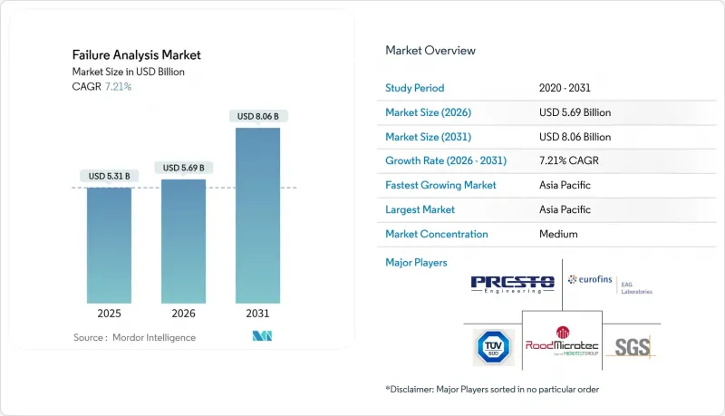
預計故障分析市場將從 2025 年的 53.1 億美元成長到 2026 年的 56.9 億美元,到 2031 年將達到 80.5 億美元,2026 年至 2031 年的複合年成長率為 7.18%。
半導體製造領域對精密診斷的需求不斷成長,老化的工業基礎設施需要更深入的檢測程序,以及傳統測試方法解析度不足的奈米裝置的穩步發展,共同推動了半導體產業的持續成長。在美國《晶片製造與資訊安全法案》(CHIPS Act)以及其他國家類似措施的推動下,供應鏈在地化進程顯著加快,促使晶圓廠內部建立分析實驗室,並由此催生了對緊湊型自動化工具的相應需求。設備供應商正積極回應,推出雙束平台和人工智慧輔助工作流程,以縮短根本原因偵測週期。同時,石油和天然氣等資產密集型產業正在採用預測性維護通訊協定,以減少代價高昂的停機時間。亞太地區在政府補貼和密集的晶圓代工廠網路的支持下,仍然是資本投資的中心。北美則正利用政策獎勵將產能回流,並加強智慧財產權管理。
全球故障分析市場趨勢與洞察
基礎設施老化和維護需求不斷增加
腐蝕相關的故障每年給石油和天然氣行業造成13.72億美元的損失,促使營運商採用預測性故障分析程序,以便在計劃外停機前檢測到劣化。深度學習驅動的有限元素模型現已被納入管道健康管理流程,取代了耗時的人工檢查,並縮短了惡劣運作環境的診斷時間。類似的趨勢也出現在老化離散製造設備領域,奈米級材料分析正被用於延長設備壽命並防止數百萬美元的生產中斷。公共產業、煉油廠和交通基礎設施所有者正擴大將掃描電子顯微鏡納入計劃維護中,這表明工業資產使用壽命的延長正在推動整個故障分析市場持續成長的需求。
故障分析工具的技術進步
人工智慧輔助影像識別技術如今可在數分鐘內分割複雜的缺陷模式,將分析週期從數週縮短至數小時。蔡司展示了一款自動化的交叉光束聚焦離子束掃描電子顯微鏡(FIB-SEM),可自主處理、成像和分類3D NAND堆疊中的缺陷,將傳統週轉時間縮短了60%。 TESCAN在台灣的擴張進一步凸顯了設備製造商向需要亞10奈米解析度的先進封裝技術領域的拓展。設備內建的即時分析功能可實現生產線內製程視窗的即時校正,從而有效地將故障分析從獨立實驗室轉移到生產現場。檢測器、離子柱和高亮度光源的進步在不影響解析度的前提下擴展了視野,並促進了多模態工作流程的實現,從而在一次掃描中整合二次離子和X光光譜測量。
設備的安裝和維修成本高昂
最先進的雙束FIB-SEM儀器造價高達數百萬美元,需要配備嚴格環境控制的隔振室。再加上維護、耗材和設備維修的成本,其終身投資金額將會翻倍。預算緊張的公司通常會選擇外包,但這可能導致物流延誤和保密問題。為了解決這些問題,儀器供應商提案模組化系統、共用設施經營模式和訂閱所有權結構,以分散資本支出並普及使用。
細分市場分析
到2025年,二次離子質譜(SIMS)將佔據失效分析市場28.85%的佔有率,主要得益於其摻雜劑分析能力,精度可提升至奈米級。聚焦離子束(FIB)工具的失效分析市場規模預計將以8.36%的複合年成長率成長,這主要受3D裝置診斷中對特定位置截面分析的需求所驅動。將SIMS、能量色散X光光譜(EDX)和飛行時間質譜(TOF-MS)整合於同一階段的混合平台可縮短工作流程步驟並提高資料相關性。新興的相對離子蝕刻技術可滿足微機電系統(MEMS)和先進材料計劃對深度分辨成分分析的需求,且不會產生掩模偽影。未來五年,人工智慧輔助的常規光譜資料解讀將使其應用範圍擴展至中型晶圓廠,從而擴大SIMS的潛在用戶群,同時增強FIB在自動化缺陷隔離方面的優勢。
3D封裝技術的日益普及也將推動對掃描探針調查方法的需求,尤其是在量子裝置開發領域,原子級表面精度至關重要。隨著光電進入量產階段,紫外線雷射輔助二次離子質譜(SIMS)將負責繪製弱訊號缺陷圖譜。結合技術多元化,預計這將使失效分析市場保持兩位數的設備更新周期,從而建立永續的投資基礎。
區域分析
預計到2025年,亞太地區將佔全球收入的46.72%,並在2031年之前以7.89%的複合年成長率成長,這主要得益於該地區集中的晶圓代工廠能力以及旨在實現半導體自給自足的政府補貼。日本已累計3.9兆日圓(約257億美元)擴大國內產能,將刺激該地區對設備部署和專業服務的需求。儘管面臨出口限制的阻力,中國的本土化策略仍在支撐來自國內供應商和國際供應商的需求。韓國在記憶體領域的主導以及台灣在先進邏輯元件領域的主導地位,為下一代分析平台的穩定採購提供了保障。
北美排名第二,《晶片與科學法案》提供的520億美元津貼和稅收優惠鼓勵新建晶圓廠在規劃階段就建立內部故障分析實驗室。五大湖區和美國西南部電動車供應鏈的成長進一步推動了該地區對功率元件可靠性研究的需求。歐洲緊追在後,德國的汽車和工業自動化產業叢集的採用率很高。 ISO 9001認證正在推動系統性的缺陷預防流程。在中東和非洲,新的需求正在湧現,主要與石油和天然氣管道完整性計劃以及在沙烏地阿拉伯「2030願景」半導體中心計劃等框架下構建半導體生態系統的早期舉措有關。雖然南美市場規模仍然小規模,但採礦設備故障診斷和可再生能源組件分析等領域的蓬勃發展正促使跨國工具供應商探索分銷合作夥伴關係。
其他福利:
- Excel格式的市場預測(ME)表
- 分析師支持(3個月)
目錄
第1章 引言
- 研究假設和市場定義
- 調查範圍
第2章調查方法
第3章執行摘要
第4章 市場情勢
- 市場概覽
- 市場促進因素
- 基礎設施老化和維護需求不斷增加
- 故障分析工具的技術進步
- 材料、設計和生產方法的創新
- 電子元件的小型化正在推動需求成長。
- 基於人工智慧的根本原因分析的採用現狀
- 供應鏈本地化促進了企業內部葉酸檢測實驗室的建立。
- 市場限制
- 設備的購置和擁有成本高昂
- 工廠自動化專業技術人員短缺
- 過長的周轉時間會阻礙生產力。
- 智慧財產權保護限制了跨境樣本共用。
- 產業價值鏈分析
- 監管環境
- 技術展望
- 波特五力分析
- 供應商的議價能力
- 買方的議價能力
- 新進入者的威脅
- 替代品的威脅
- 競爭對手之間的競爭
- 對宏觀經濟趨勢的市場評估
第5章 市場規模與成長預測
- 透過技術
- 二次電離質譜法(SIMS)
- 能量色散X光光譜(EDX)
- 化學機械拋光(CMP)
- 掃描探針顯微鏡
- 聚焦離子束(FIB)
- 相對離子蝕刻(RIE)
- 其他技術
- 透過裝置
- 掃描電子顯微鏡(SEM)
- 聚焦離子束(FIB)系統
- 穿透式電子顯微鏡(TEM)
- 雙束系統
- 其他設備
- 按最終用戶行業分類
- 車
- 石油和天然氣
- 防禦
- 建造
- 製造業
- 電子裝置和半導體
- 其他終端用戶產業
- 按地區
- 北美洲
- 美國
- 加拿大
- 墨西哥
- 南美洲
- 巴西
- 阿根廷
- 南美洲其他地區
- 歐洲
- 德國
- 英國
- 法國
- 義大利
- 西班牙
- 其他歐洲
- 亞太地區
- 中國
- 日本
- 印度
- 新加坡
- 澳洲
- 馬來西亞
- 亞太其他地區
- 中東和非洲
- 中東
- 沙烏地阿拉伯
- 阿拉伯聯合大公國
- 其他中東地區
- 非洲
- 南非
- 埃及
- 其他非洲地區
- 中東
- 北美洲
第6章 競爭情勢
- 市場集中度
- 策略趨勢
- 市佔率分析
- 公司簡介
- Presto Engineering Inc.
- TUV SUD
- Rood Microtec GmbH
- Eurofins EAG Laboratories
- SGS SA
- CoreTest Technologies Inc.
- Materials Testing Inc.
- McDowell Owens Engineering Inc.
- Exponent Inc.
- TechInsights Inc.
- Hitachi High-Tech Analytical Science Ltd.
- Intertek Group plc
- NanoScope Services Ltd
- Applus+Laboratories Inc.
- Advanced Nanolab Pte Ltd
- Toray Engineering Co., Ltd.
- Tescan Orsay Holding
- Leica Microsystems Inc.
- Keysight Technologies Inc.
- Crane Engineering Inc.
第7章 市場機會與未來展望
The Failure Analysis market is expected to grow from USD 5.31 billion in 2025 to USD 5.69 billion in 2026 and is forecast to reach USD 8.05 billion by 2031 at 7.18% CAGR over 2026-2031.
Persistent growth rests on rising precision-diagnostics demand in semiconductor manufacturing, aging industrial infrastructure that mandates deeper inspection routines, and the steady shift to nanoscale devices where conventional test methods lose resolution. Intensifying supply-chain localization, most visibly under the U.S. CHIPS Act and similar initiatives elsewhere, accelerates in-house analytical-lab adoption inside fabs, creating parallel demand for compact, automated tools. Equipment vendors are responding with dual-beam platforms and AI-assisted workflows that shorten root-cause cycles, while asset-heavy sectors such as oil and gas adopt predictive protocols to curb costly downtime events. Asia-Pacific remains the epicenter of capital expenditure, helped by government subsidies and its dense foundry network, whereas North America leverages policy incentives to reshore capacity and tighten intellectual-property control.
Global Failure Analysis Market Trends and Insights
Ageing Infrastructure and Increasing Maintenance Needs
Corrosion-related failures cost the oil and gas sector USD 1.372 billion each year, a burden that is steering operators toward predictive failure analysis programs that detect degradation before unplanned shutdowns. Deep-learning-enabled finite-element models are now embedded into pipeline-integrity routines, replacing slower manual inspections and cutting diagnostic time in harsh operating zones. Similar patterns appear in aging discrete-manufacturing equipment, where nanoscale materials analysis helps extend tool life and prevent multi-million-dollar production halts. Utilities, refineries, and transportation infrastructure owners increasingly embed scanning-electron-microscopy checks in scheduled maintenance, illustrating how industrial asset longevity fuels recurring demand across the failure analysis market.
Technological Advancements in Failure-Analysis Tools
AI-assisted image-recognition now segments complex defect patterns in minutes, slashing analysis-cycle time from weeks to hours. ZEISS demonstrated an automated Crossbeam FIB-SEM that can autonomously mill, image, and classify faults in 3D NAND stacks, shaving 60% off typical turnaround schedules. TESCAN's expansion in Taiwan further underscores toolmakers' push into advanced-packaging nodes that require resolution below 10 nm. Real-time analytics embedded directly on the tool allow immediate process-window corrections inside fab lines, effectively relocating failure analysis from separate laboratories to production floors. Advancements in detectors, ion columns, and high-brightness sources also extend the field-of-view without compromising resolution, fostering multimodal workflows that merge secondary-ion and X-ray spectrometry in a single pass.
High Acquisition and Ownership Cost of Equipment
A state-of-the-art dual-beam FIB-SEM can command several million USD and requires vibration-isolated rooms with strict environmental controls, doubling the lifetime investment once maintenance, consumables, and facility retrofits are factored in. Budget-constrained enterprises often resort to outsourcing, introducing logistics delays and potential confidentiality issues. Tool vendors are countering with modular systems, shared-facility business models, and subscription-based ownership structures that spread capital outlays and democratize access.
Other drivers and restraints analyzed in the detailed report include:
- Innovation in Materials, Design and Production Methods
- Miniaturization of Electronic Components Boosts Demand
- Shortage of Skilled Failure Analysis Professionals
For complete list of drivers and restraints, kindly check the Table Of Contents.
Segment Analysis
SIMS held 28.85% of the failure analysis market share in 2025, favored for dopant-profiling accuracy that scales into single-digit nanometers. The failure analysis market size tied to Focused Ion Beam tools is on course for an 8.36% CAGR, propelled by demand for site-specific cross-sectioning during 3D-device diagnostics. Hybrid platforms that merge SIMS, EDX, and time-of-flight mass spectrometry on the same stage now shorten workflow steps and improve data correlation. Emerging Relative Ion Etching complements MEMS and advanced-materials projects that need depth-resolved compositional profiling without masking artifacts. Over the next five years, AI-assisted routine-spectra interpretation will extend usability to mid-tier fabs, expanding the addressable base for SIMS while reinforcing FIB traction in automated defect isolation.
Wider 3D packaging adoption also lifts scanning-probe methodologies, especially for quantum-device development that hinges on atomic-scale surface fidelity. As photonics-integrated circuits enter mass production, ultraviolet laser-assisted SIMS steps in to map low-signal defects. Collectively, technology diversification will sustain double-digit tool refresh cycles and anchor continuous investment in the failure analysis market.
The Failure Analysis Market Report is Segmented by Technology (Secondary ION Mass Spectrometry, Energy Dispersive X-Ray Spectroscopy, and More), Equipment (Scanning Electron Microscope, Focused Ion Beam System, and More), End-User Industry (Automotive, Oil and Gas, and More), and Geography (North America, South America, Europe, Asia-Pacific, and Middle East and Africa). The Market Forecasts are Provided in Terms of Value (USD).
Geography Analysis
Asia-Pacific held 46.72% of global revenue in 2025 and is forecast to grow at 7.89% CAGR through 2031, bolstered by concentrated foundry capacity and national subsidies that target semiconductor self-sufficiency. Japan earmarked JPY 3.9 trillion (USD 25.7 billion) to lift domestic output, sparking a surge in regional tool installations and specialized-service inquiries. China's localization strategy keeps domestic tool vendors and overseas suppliers occupied, even amid export-control headwinds. South Korea's memory leadership and Taiwan's advanced-logic dominance reinforce steady procurement of next-generation analytical platforms.
North America ranks second as the CHIPS and Science Act allocates USD 52 billion in grants and tax incentives, motivating new fabs that embed in-house failure analysis laboratories during planning phases. Electric-vehicle supply-chain growth around the Great Lakes and U.S. Southwest further increases regional demand for power-device reliability studies. Europe follows with strong adoption in Germany's automotive and industrial-automation clusters, where ISO 9001 compliance drives systematic defect-prevention cycles. Middle East and Africa exhibit emerging traction, primarily tied to oil-and-gas pipeline integrity programs and early moves to build semiconductor ecosystems under policy umbrellas such as Saudi Arabia's Vision 2030 semiconductor hub. South America remains a smaller market but shows promise in mining-equipment fault diagnostics and renewable-energy component analysis, leading multinational tool vendors to explore distributor partnerships
- Presto Engineering Inc.
- TUV SUD
- Rood Microtec GmbH
- Eurofins EAG Laboratories
- SGS SA
- CoreTest Technologies Inc.
- Materials Testing Inc.
- McDowell Owens Engineering Inc.
- Exponent Inc.
- TechInsights Inc.
- Hitachi High-Tech Analytical Science Ltd.
- Intertek Group plc
- NanoScope Services Ltd
- Applus+ Laboratories Inc.
- Advanced Nanolab Pte Ltd
- Toray Engineering Co., Ltd.
- Tescan Orsay Holding
- Leica Microsystems Inc.
- Keysight Technologies Inc.
- Crane Engineering Inc.
Additional Benefits:
- The market estimate (ME) sheet in Excel format
- 3 months of analyst support
TABLE OF CONTENTS
1 INTRODUCTION
- 1.1 Study Assumptions and Market Definition
- 1.2 Scope of the Study
2 RESEARCH METHODOLOGY
3 EXECUTIVE SUMMARY
4 MARKET LANDSCAPE
- 4.1 Market Overview
- 4.2 Market Drivers
- 4.2.1 Ageing infrastructure and increasing maintenance needs
- 4.2.2 Technological advancements in failure-analysis tools
- 4.2.3 Innovation in materials, design and production methods
- 4.2.4 Miniaturisation of electronic components boosts demand
- 4.2.5 AI-driven root-cause analytics adoption
- 4.2.6 Supply-chain localization spurs in-house FA labs
- 4.3 Market Restraints
- 4.3.1 High acquisition and ownership cost of equipment
- 4.3.2 Shortage of skilled FA professionals
- 4.3.3 Long turnaround time hampers productivity
- 4.3.4 IP-protection limits cross-border sample sharing
- 4.4 Industry Value Chain Analysis
- 4.5 Regulatory Landscape
- 4.6 Technological Outlook
- 4.7 Porter's Five Forces Analysis
- 4.7.1 Bargaining Power of Suppliers
- 4.7.2 Bargaining Power of Buyers
- 4.7.3 Threat of New Entrants
- 4.7.4 Threat of Substitutes
- 4.7.5 Intensity of Competitive Rivalry
- 4.8 Assessment of Macro-economic Trends on the Market
5 MARKET SIZE AND GROWTH FORECASTS (VALUE)
- 5.1 By Technology
- 5.1.1 Secondary ION Mass Spectrometry (SIMS)
- 5.1.2 Energy Dispersive X-ray Spectroscopy (EDX)
- 5.1.3 Chemical Mechanical Planarization (CMP)
- 5.1.4 Scanning Probe Microscopy
- 5.1.5 Focused Ion Beam (FIB)
- 5.1.6 Relative Ion Etching (RIE)
- 5.1.7 Other Technologies
- 5.2 By Equipment
- 5.2.1 Scanning Electron Microscope (SEM)
- 5.2.2 Focused Ion Beam (FIB) System
- 5.2.3 Transmission Electron Microscope (TEM)
- 5.2.4 Dual Beam System
- 5.2.5 Other Equipment's
- 5.3 By End-user Industry
- 5.3.1 Automotive
- 5.3.2 Oil and Gas
- 5.3.3 Defense
- 5.3.4 Construction
- 5.3.5 Manufacturing
- 5.3.6 Electronics and Semiconductors
- 5.3.7 Other End-user Industries
- 5.4 By Geography
- 5.4.1 North America
- 5.4.1.1 United States
- 5.4.1.2 Canada
- 5.4.1.3 Mexico
- 5.4.2 South America
- 5.4.2.1 Brazil
- 5.4.2.2 Argentina
- 5.4.2.3 Rest of South America
- 5.4.3 Europe
- 5.4.3.1 Germany
- 5.4.3.2 United Kingdom
- 5.4.3.3 France
- 5.4.3.4 Italy
- 5.4.3.5 Spain
- 5.4.3.6 Rest of Europe
- 5.4.4 Asia-Pacific
- 5.4.4.1 China
- 5.4.4.2 Japan
- 5.4.4.3 India
- 5.4.4.4 Singapore
- 5.4.4.5 Australia
- 5.4.4.6 Malaysia
- 5.4.4.7 Rest of Asia-Pacific
- 5.4.5 Middle East and Africa
- 5.4.5.1 Middle East
- 5.4.5.1.1 Saudi Arabia
- 5.4.5.1.2 United Arab Emirates
- 5.4.5.1.3 Rest of Middle East
- 5.4.5.2 Africa
- 5.4.5.2.1 South Africa
- 5.4.5.2.2 Egypt
- 5.4.5.2.3 Rest of Africa
- 5.4.5.1 Middle East
- 5.4.1 North America
6 COMPETITIVE LANDSCAPE
- 6.1 Market Concentration
- 6.2 Strategic Moves
- 6.3 Market Share Analysis
- 6.4 Company Profiles (includes Global level Overview, Market level overview, Core Segments, Financials as available, Strategic Information, Market Rank/Share for key companies, Products and Services, and Recent Developments)
- 6.4.1 Presto Engineering Inc.
- 6.4.2 TUV SUD
- 6.4.3 Rood Microtec GmbH
- 6.4.4 Eurofins EAG Laboratories
- 6.4.5 SGS SA
- 6.4.6 CoreTest Technologies Inc.
- 6.4.7 Materials Testing Inc.
- 6.4.8 McDowell Owens Engineering Inc.
- 6.4.9 Exponent Inc.
- 6.4.10 TechInsights Inc.
- 6.4.11 Hitachi High-Tech Analytical Science Ltd.
- 6.4.12 Intertek Group plc
- 6.4.13 NanoScope Services Ltd
- 6.4.14 Applus+ Laboratories Inc.
- 6.4.15 Advanced Nanolab Pte Ltd
- 6.4.16 Toray Engineering Co., Ltd.
- 6.4.17 Tescan Orsay Holding
- 6.4.18 Leica Microsystems Inc.
- 6.4.19 Keysight Technologies Inc.
- 6.4.20 Crane Engineering Inc.
7 MARKET OPPORTUNITIES AND FUTURE OUTLOOK
- 7.1 White-space and Unmet-Need Assessment
 失效測試與分析服務市場:依服務類型、技術、材料類型、最終用戶產業與應用分類-2026-2032年全球預測
 2026年全球失效分析市場報告故障調查服務市場:依服務模式、調查方法、組件類型、產業垂直領域和最終用戶分類-2026-2032年全球預測按產品類型、最終用戶、分銷管道、應用和技術分類的故障分析市場 - 全球預測 2025-2032
 全球失效分析與測試設備市場:市場規模、佔有率和趨勢分析(按產品、技術、應用和地區分類),細分市場預測(2025-2033 年)
 2025 年至 2033 年故障分析市場規模、佔有率、趨勢及預測(按設備、最終用途、產業及地區)
 故障分析市場:2025-2030 年預測半導體故障分析設備市場規模、佔有率、趨勢分析報告:產品、技術、地區、細分市場預測,2025-2030
 故障分析設備市場規模、佔有率、成長分析,按設備類型、按技術、按應用、按最終用戶、按地區 - 行業預測,2025 年至 2032 年故障分析市場規模、佔有率、趨勢分析報告:2024-2030 年按設備、技術、產業、地區和細分市場進行的預測