


 |
市場調查報告書
商品編碼
1906136
光阻劑:市場佔有率分析、產業趨勢與統計、成長預測(2026-2031)Photoresist - Market Share Analysis, Industry Trends & Statistics, Growth Forecasts (2026 - 2031) |
||||||
※ 本網頁內容可能與最新版本有所差異。詳細情況請與我們聯繫。
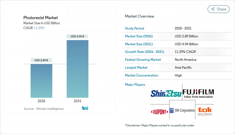
預計到 2025 年,光阻劑市場價值將達到 26 億美元,到 2031 年將達到 49.4 億美元,高於 2026 年的 28.9 億美元。
預計在預測期(2026-2031 年)內,複合年成長率將達到 11.29%。
推動這項擴張的因素包括:極紫外線 (EUV) 光刻技術在亞10奈米特徵尺寸製造中的廣泛應用、人工智慧 (AI) 加速器需求的激增以及政府主導的晶圓廠激勵措施。台灣、韓國和美國的半導體製造商正擴大採用抗蝕劑高 EUV 吸收率和低線邊緣粗糙度的金屬氧化物和光阻劑,從而提高生產效率並降低每層抗蝕劑的使用量。 5G 和物聯網 (IoT) 設備的同步發展也持續推動成熟節點對 G 線、I 線和 KrF 材料的需求。同時,晶片組、扇出型晶圓層次電子構裝和光學共封裝等先進封裝結構需要與銅柱和矽通孔 (TSV) 結構相容的厚膜抗蝕劑。供應鏈風險仍然較高,三家日本製造商佔據了先進抗蝕劑的約 60%,促使北美和歐洲的製造商進行地域多角化,並提高本地產能。
全球光阻劑市場趨勢及展望
來自半導體和人工智慧加速器的需求不斷成長
目前,晶片製造商為大規模語言模型訓練和推理工作負載生產硬體時,通常會在每個裝置上整合多個線路重布、中介層和矽通孔(TSV)。 NVIDIA 的 H100 和即將推出的 Blackwell 系列採用晶片組佈局,其每個成品裝置的光阻劑消耗量是傳統單晶片 GPU 的三到五倍。台積電(TSMC)擴大其晶片封裝(CoWoS)產能,推動了對厚度達 50 微米的抗蝕劑的需求。同時,先進的銅柱電鍍技術採用針對 3:1 或更大長寬比最佳化的負性光阻配方。產能擴張最初將在台灣和韓國進行,預計到 2027 年將擴展到美國的新晶圓廠。
加速EUV微影術應用與高數值孔徑藍圖
ASML 的 0.55NA EUV 曝光工具可實現 8nm 間距的單次曝光圖形化,無需高成本的多次圖形化步驟。為了滿足更嚴格的線邊緣粗糙度目標(小於 1.5nm),晶圓廠採用了基於鉿鋯叢集的金屬氧化物抗蝕劑,其 EUV 光吸收效率是有機抗蝕劑的九倍。這使得曝光劑量從 40 mJ/cm² 降低到小於 20 mJ/cm²,從而提高了生產效率並降低了單片晶圓的成本。根據 2025 年在三星平澤生產線進行的試點運行結果,預計 2026 年在 2nm 製程節點上實現商業部署。
關於溶劑和光酸發生器的嚴格健康、安全和環境 (HSE) 法規
2024年,歐盟修訂了2024/573號法規,計畫在2045年逐步淘汰90%的氫氟碳化合物。目前,許多極紫外光光阻劑使用全氟化光酸發生劑和溶劑,這些物質需要經過註冊、評估和批准。合規要求對雜質含量低於1 ppb進行分析檢驗,這增加了品管成本,並迫使配方師測試替代化學方法,而這會帶來性能下降的風險。
細分市場分析
受台積電、三星和英特爾等廠商對7nm和5nm製程的持續需求推動,ArF浸沒式光阻劑預計在2025年將維持31.85%的光阻劑市場佔有率。同時,隨著晶圓廠向2nm邏輯製程轉型,金屬氧化物抗蝕劑和EUV乾式抗蝕劑預計將創造最大的增量價值,年複合成長率將達到12.94%。鉿基叢集的抗蝕刻性能是普通有機聚合物的25倍以上,無需硬掩模即可直接轉移到介電層,從而縮短製程。
Lam Research 的乾式沉積光阻抗蝕劑消除旋塗製程的廢棄物,並將化學品消費量降低高達 90%。該平台計劃於 2026 年實現量產,預計將材料收入從濕化學品供應商轉移到設備整合供應商。 KrF、G 系列和 I 系列抗蝕劑在汽車和工業領域仍然至關重要,隨著先進製程節點推動成長,它們將為公司提供穩定的基礎收入。
到 2025 年,正性光阻材料佔光阻劑市場的 71.45%。負性抗蝕劑,尤其是環氧樹脂和金屬氧化物基光阻,預計到 2031 年將以 11.38% 的複合年成長率成長,這主要得益於先進封裝中對更厚薄膜層的需求激增。
負性抗蝕劑能夠承受銅柱電鍍過程中的高電流密度,從而實現長寬比,這對於形成小間距凸塊至關重要。新興的雙色調氧化錫平台透過劑量控制的色調切換,提供了製程柔軟性。 imec的初步測試表明,在20mJ/cm²的曝光劑量下,解析度可低於16nm。
區域分析
預計到2025年,亞太地區在全球營收中所佔佔有率將達到72.10%,這主要得益於台灣和韓國高密度邏輯晶片產能的擴張,以及中國成熟節點晶圓廠的建設。台積電面向高效能運算的2nm製程量產和封裝生產線推動了EUV光阻和厚膜材料的消費量成長,而三星的3D NAND快閃記憶體產能則帶動了對高選擇性KrF抗蝕劑的需求。日本的設備生態系統、東京電子的鍍膜設備以及尼康的步進光刻機為日本國內供應商提供了支持,形成了一條緊密整合的供應鏈。
在北美,《晶片製造和整合法案》(CHIPS Act)的實施將促進新建待開發區的建設,預計到2031年,其年複合成長率將達到11.49%。到2028年,英特爾位於俄亥俄州的園區、台積電位於亞利桑那州的工廠以及三星位於德克薩斯州的工廠將總合超過30萬晶圓/分鐘的先進產能,以滿足該地區對抗蝕劑及相關化學品的需求。杜邦位於科羅拉多的擴建項目和陶氏位於密西根州的擴建項目旨在為該地區提供產品,並降低跨太平洋物流風險。
在歐洲,嚴格遵守REACH法規將推高配方成本,而英特爾在愛爾蘭的大規模投資以及在德國的建設計畫計畫將起到推動作用。當地材料供應商默克集團和BASF正利用其在法規方面的專業知識,為EUV生產線爭取認證。東歐國家則致力於吸引封裝和測試業務,以實現地理佈局的多元化。
中東、非洲和南美洲是發展中地區,但它們正在大力推動先進封裝和微機電系統(MEMS)製造,尤其是在電信基地台和汽車感測器領域。這些地區政府提供稅收優惠以吸引後端組裝,從而提振了對G線和I線工藝光阻劑的需求,但先進製程節點仍集中在其他地區。
其他福利:
- Excel格式的市場預測(ME)表
- 分析師支持(3個月)
目錄
第1章 引言
- 研究假設和市場定義
- 調查範圍
第2章調查方法
第3章執行摘要
第4章 市場情勢
- 市場概覽
- 市場促進因素
- 來自半導體和人工智慧加速器的需求不斷成長
- 加速採用EUV微影技術及高數值孔徑藍圖
- 由於5G/物聯網設備的廣泛應用,晶圓產量增加。
- 政府晶圓廠獎勵計畫(美國/歐盟晶片法案)
- 乾式沉積金屬氧化物抗蝕劑可提高極紫外光刻效率
- 市場限制
- 溶劑和光酸發生器的嚴格健康、安全和環境法規
- 供應鏈集中度與出口管制風險
- 逐步淘汰歐盟REACH法規和針對含氟溶劑的氟碳法規
- 價值鏈分析
- 監管環境
- 波特五力模型
- 供應商的議價能力
- 買方的議價能力
- 新進入者的威脅
- 替代品的威脅
- 競爭程度
第5章 市場規模與成長預測
- 抗蝕劑類型
- ArF浸入式
- ArF 乾式
- KrF
- G-Line
- I 線
- 用於極紫外光刻的金屬氧化物和乾式抗蝕劑
- 其他類型
- 按音調
- 積極的
- 消極的
- 透過使用
- 半導體和積體電路(IC)
- 先進封裝(扇出型 WLP、RDL)
- 平板顯示器(LCD/ 有機發光二極體)
- 印刷基板
- 微機電系統和感測器
- 其他用途
- 按最終用戶行業分類
- 電子電器設備
- 汽車與出行
- 航太/國防
- 消費品(包裝)
- 其他行業
- 按地區
- 亞太地區
- 中國
- 日本
- 韓國
- 台灣
- 印度
- 亞太其他地區
- 北美洲
- 美國
- 加拿大
- 墨西哥
- 歐洲
- 德國
- 英國
- 法國
- 義大利
- 俄羅斯
- 其他歐洲地區
- 南美洲
- 巴西
- 阿根廷
- 南美洲其他地區
- 中東和非洲
- 沙烏地阿拉伯
- 阿拉伯聯合大公國
- 南非
- 其他中東和非洲地區
- 亞太地區
第6章 競爭情勢
- 市場集中度
- 策略趨勢
- 市佔率(%)/排名分析
- 公司簡介
- ALLRESIST GmbH
- Asahi Kasei Corporation
- Avantor, Inc.
- Brewer Science, Inc.
- DJ MicroLaminates
- DONGJIN SEMICHEM CO. LTD
- DuPont
- Eternal Materials Co., Ltd.
- FUJIFILM Corporation
- Inpria
- JSR Corporation
- SEMI
- Kolon Industries, Inc.
- LG Chem
- Merck KGaA
- micro resist technology GmbH
- Microchemicals GmbH
- Shin-Etsu Chemical Co., Ltd.
- Sumitomo Chemical Co., Ltd.
- TOKYO OHKA KOGYO CO., LTD.
- Jiangsu Nata Opto-electronic Material Co., Ltd.
第7章 市場機會與未來展望
The Photoresist Market was valued at USD 2.60 billion in 2025 and estimated to grow from USD 2.89 billion in 2026 to reach USD 4.94 billion by 2031, at a CAGR of 11.29% during the forecast period (2026-2031).
The widespread deployment of extreme-ultraviolet (EUV) lithography at sub-10-nanometer dimensions, the fast-growing demand for artificial-intelligence (AI) accelerators, and government-funded fab incentives underpin this expansion. Semiconductor manufacturers in Taiwan, South Korea, and the United States are increasingly favoring metal-oxide and dry photoresists that deliver higher EUV absorption and lower line-edge roughness, thereby boosting throughput and reducing per-layer resist usage. Parallel momentum in 5G and Internet-of-Things (IoT) devices sustains demand for mature-node G-line, I-line, and KrF materials. Meanwhile, advanced packaging architectures-such as chiplets, fan-out wafer-level packaging, and co-packaged optics-require thick-film resists that are compatible with copper pillar and through-silicon-via (TSV) structures. Supply-chain risks remain elevated because three Japanese suppliers collectively account for roughly 60% of advanced resists, prompting regional diversification and localized capacity additions in North America and Europe.
Global Photoresist Market Trends and Insights
Growing Demand from Semiconductor and AI Accelerators
Chipmakers producing hardware for training large language models and powering inference workloads now pattern multiple redistribution layers, interposers, and TSVs for each device. NVIDIA's H100 and forthcoming Blackwell series adopt chiplet layouts that consume three to five times more photoresist per finished part than previous monolithic GPUs. Taiwan Semiconductor Manufacturing Company's (TSMC) expansion of CoWoS capacity lifts thick-film resist of up to 50 µm, while advanced copper pillar plating uses negative-tone formulations optimized for aspect ratios above 3:1. Volume gains occur first in Taiwan and South Korea but ripple into new fabs in the United States by 2027.
Accelerated EUV Lithography Adoption and High-NA Roadmap
ASML's 0.55-NA EUV scanners enable single-exposure patterning with an 8 nm pitch, eliminating costly multiple-patterning steps. To meet the tighter line-edge roughness target of below 1.5 nm, fabs qualify metal-oxide resists based on hafnium and zirconium clusters that absorb EUV 9 times more effectively than organic formulations . The dose can be reduced from 40 mJ/cm2 to sub-20 mJ/cm2, increasing throughput and lowering the cost per wafer. Pilot runs at Samsung's Pyeongtaek lines in 2025 suggest commercial adoption at 2 nm nodes in 2026.
Stringent HSE Regulations on Solvents and Photo-Acid Generators
The European Union's 2024 revision to Regulation (EU) 2024/573 schedules a phase-down of hydrofluorocarbon usage by 90% before 2045. Many EUV photoresists now employ perfluorinated photoacid generators and solvents, which are subject to registration, evaluation, and authorization. Compliance requires analytical verification of impurity levels below 1 ppb, which drives up quality-control costs and forces formulators to test alternative chemistries that may risk lower performance.
Other drivers and restraints analyzed in the detailed report include:
- 5G/IoT Device Proliferation Expanding Wafer Starts
- Government Fab-Incentive Programs (US/EU Chips Acts)
- Supply-Chain Concentration and Export-Control Exposure
For complete list of drivers and restraints, kindly check the Table Of Contents.
Segment Analysis
ArF immersion formulations retained a 31.85% share of the photoresist market size in 2025, thanks to sustained demand for 7 nm and 5 nm volumes at TSMC, Samsung, and Intel. Conversely, EUV metal-oxide and dry resists are projected to post a 12.94% CAGR, generating the largest incremental value as fabs transition to 2 nm logic. Hafnium-based clusters deliver etch resistance exceeding 25 times that of organic polymers, enabling direct transfer into dielectric layers without a hard mask and thus shortening the process flow.
Lam Research's dry-deposited resist eliminates spin waste and cuts chemical consumption by up to 90%. With mass production targeted for 2026, this platform could shift material revenue from wet-chemistry suppliers toward equipment-integrated delivery. KrF, G-line, and I-line resists remain essential for automotive and industrial nodes, anchoring a steady base revenue even as advanced nodes dominate growth.
Positive-tone materials dominated the photoresist market with a 71.45% share in 2025. Negative-tone resists, particularly epoxy-based and metal-oxide systems, are forecast to rise at 11.38% CAGR through 2031 as demand for high-thickness layers in advanced packaging surges.
Negative resists withstand high current densities during copper-pillar plating and achieve aspect ratios exceeding 3:1, which is critical for fine-pitch bump formation. Emerging dual-tone tin-oxide platforms offer process flexibility by switching tone with dose control; early tests at imec show sub-16 nm resolution at 20 mJ/cm2 exposure.
The Photoresist Market Report is Segmented by Resist Type (ArF Immersion and More), Tone (Positive and Negative), Application (Semiconductors and ICs and More), End-User Industry (Electronics and Electricals and More), and Geography (Asia-Pacific, North America, Europe, South America, and Middle-East and Africa). The Market Forecasts are Provided in Terms of Value (USD).
Geography Analysis
The Asia-Pacific region accounted for 72.10% of global revenue in 2025, driven by dense logic capacity in Taiwan and South Korea, as well as the expansion of mature-node fabs in China. TSMC's 2nm ramp and high-performance computing package lines consume increasing volumes of EUV and thick-film materials, while Samsung's 3D NAND capacity drives demand for high-selectivity KrF resists. Japan's equipment ecosystem, Tokyo Electron coating tracks, and Nikon steppers, support domestic suppliers, creating a tightly integrated supply chain.
North America is forecast to record an 11.49% CAGR through 2031 as the CHIPS Act stimulates the construction of new greenfield fabs. Intel's Ohio campus, TSMC's Arizona site, and Samsung's Texas facility together add more than 300,000 wpm of leading-edge capacity by 2028, underpinning local resist and ancillary chemical demand. DuPont's Colorado expansion and Dow's Michigan expansion aim to supply the region and reduce trans-Pacific logistics risk.
Europe faces stringent REACH compliance, which raises formulation costs, yet benefits from Intel's large-scale investment in Ireland and prospective fabs in Germany. Local material suppliers, Merck KGaA and BASF, utilize their regulatory expertise to secure qualification for EUV lines. Eastern European countries court packaging and test operations, further diversifying the regional footprint.
Middle East & Africa and South America remain nascent but pursue specialty packaging and MEMS manufacturing, particularly for telecom base-stations and automotive sensors. Regional governments offer tax credits to attract backend assembly, bringing incremental photoresist volumes for G-line and I-line processes while advanced nodes stay concentrated elsewhere.
- ALLRESIST GmbH
- Asahi Kasei Corporation
- Avantor, Inc.
- Brewer Science, Inc.
- DJ MicroLaminates
- DONGJIN SEMICHEM CO. LTD
- DuPont
- Eternal Materials Co., Ltd.
- FUJIFILM Corporation
- Inpria
- JSR Corporation
- SEMI
- Kolon Industries, Inc.
- LG Chem
- Merck KGaA
- micro resist technology GmbH
- Microchemicals GmbH
- Shin-Etsu Chemical Co., Ltd.
- Sumitomo Chemical Co., Ltd.
- TOKYO OHKA KOGYO CO., LTD.
- Jiangsu Nata Opto-electronic Material Co., Ltd.
Additional Benefits:
- The market estimate (ME) sheet in Excel format
- 3 months of analyst support
TABLE OF CONTENTS
1 Introduction
- 1.1 Study Assumptions & Market Definition
- 1.2 Scope of the Study
2 Research Methodology
3 Executive Summary
4 Market Landscape
- 4.1 Market Overview
- 4.2 Market Drivers
- 4.2.1 Growing demand from semiconductor and AI accelerators
- 4.2.2 Accelerated EUV lithography adoption and High-NA roadmap
- 4.2.3 5G / IoT device proliferation expanding wafer starts
- 4.2.4 Government fab-incentive programs (US/EU Chips Acts)
- 4.2.5 Dry-deposited metal-oxide resists boosting EUV throughput
- 4.3 Market Restraints
- 4.3.1 Stringent HSE regulations on solvents and photo-acid generators
- 4.3.2 Supply-chain concentration and export-control exposure
- 4.3.3 EU REACH and F-gas phase-outs targeting fluorinated solvents
- 4.4 Value Chain Analysis
- 4.5 Regulatory Landscape
- 4.6 Porter's Five Forces
- 4.6.1 Bargaining Power of Suppliers
- 4.6.2 Bargaining Power of Buyers
- 4.6.3 Threat of New Entrants
- 4.6.4 Threat of Substitutes
- 4.6.5 Degree of Competition
5 Market Size & Growth Forecasts (Value)
- 5.1 By Resist Type
- 5.1.1 ArF Immersion
- 5.1.2 ArF Dry
- 5.1.3 KrF
- 5.1.4 G-Line
- 5.1.5 I-Line
- 5.1.6 EUV Metal-Oxide and Dry Resists
- 5.1.7 Other Types
- 5.2 By Tone
- 5.2.1 Positive
- 5.2.2 Negative
- 5.3 By Application
- 5.3.1 Semiconductors and ICs
- 5.3.2 Advanced Packaging (Fan-Out WLP, RDL)
- 5.3.3 Flat-Panel Displays (LCD/OLED)
- 5.3.4 Printed Circuit Boards
- 5.3.5 MEMS and Sensors
- 5.3.6 Other Applications
- 5.4 By End-User Industry
- 5.4.1 Electronics and Electricals
- 5.4.2 Automotive and Mobility
- 5.4.3 Aerospace and Defense
- 5.4.4 Consumer Packaged Goods (Packaging)
- 5.4.5 Other Industries
- 5.5 By Geography
- 5.5.1 Asia-Pacific
- 5.5.1.1 China
- 5.5.1.2 Japan
- 5.5.1.3 South Korea
- 5.5.1.4 Taiwan
- 5.5.1.5 India
- 5.5.1.6 Rest of Asia-Pacific
- 5.5.2 North America
- 5.5.2.1 United States
- 5.5.2.2 Canada
- 5.5.2.3 Mexico
- 5.5.3 Europe
- 5.5.3.1 Germany
- 5.5.3.2 United Kingdom
- 5.5.3.3 France
- 5.5.3.4 Italy
- 5.5.3.5 Russia
- 5.5.3.6 Rest of Europe
- 5.5.4 South America
- 5.5.4.1 Brazil
- 5.5.4.2 Argentina
- 5.5.4.3 Rest of South America
- 5.5.5 Middle-East and Africa
- 5.5.5.1 Saudi Arabia
- 5.5.5.2 United Arab Emirates
- 5.5.5.3 South Africa
- 5.5.5.4 Rest of Middle-East and Africa
- 5.5.1 Asia-Pacific
6 Competitive Landscape
- 6.1 Market Concentration
- 6.2 Strategic Moves
- 6.3 Market Share (%)/Ranking Analysis
- 6.4 Company Profiles (includes Global-level Overview, Market-level Overview, Core Segments, Financials, Strategic Information, Market Rank/Share, Products & Services, Recent Developments)
- 6.4.1 ALLRESIST GmbH
- 6.4.2 Asahi Kasei Corporation
- 6.4.3 Avantor, Inc.
- 6.4.4 Brewer Science, Inc.
- 6.4.5 DJ MicroLaminates
- 6.4.6 DONGJIN SEMICHEM CO. LTD
- 6.4.7 DuPont
- 6.4.8 Eternal Materials Co., Ltd.
- 6.4.9 FUJIFILM Corporation
- 6.4.10 Inpria
- 6.4.11 JSR Corporation
- 6.4.12 SEMI
- 6.4.13 Kolon Industries, Inc.
- 6.4.14 LG Chem
- 6.4.15 Merck KGaA
- 6.4.16 micro resist technology GmbH
- 6.4.17 Microchemicals GmbH
- 6.4.18 Shin-Etsu Chemical Co., Ltd.
- 6.4.19 Sumitomo Chemical Co., Ltd.
- 6.4.20 TOKYO OHKA KOGYO CO., LTD.
- 6.4.21 Jiangsu Nata Opto-electronic Material Co., Ltd.
7 Market Opportunities and Future Outlook
- 7.1 White-space and Unmet-Need Assessment
 EUV光阻劑材料市場分析及預測(至2035年):依類型、產品、技術、應用、材料類型、製程、最終用戶、功能及設備分類
 2026年混合對數伽瑪(HLG)光電顯示支架全球市場報告
 IC光阻劑市場:按技術、類型、形式、基板、應用和最終用戶分類-全球預測,2026-2032年KrF光阻劑市場(半導體領域):按類型、組件、技術節點、應用和最終用戶產業分類-2026年至2032年全球預測TFT-LCD光阻劑市場:按類型、成分、曝光方法、製程、應用、最終用途和銷售管道-全球預測,2026-2032年正性光阻劑市場:按抗蝕劑類型、製程、厚度範圍、應用和最終用途產業分類-2026-2032年全球預測顯示光阻劑市場:按類型、技術、塗覆方法、應用和最終用途分類-2026-2032年全球預測KrF抗蝕劑市場按化學成分、技術節點、應用方法、應用領域和最終用戶分類-2026-2032年全球預測光阻劑市場按技術、材料類型、產品類型、波長和應用分類-2026-2032年全球預測半導體光阻劑市場:2026-2032年全球預測(按抗蝕劑類型、化學成分、技術節點、晶圓尺寸、曝光技術、產品形式和應用分類)