


 |
市場調查報告書
商品編碼
1851534
CMOS影像感測器:市場佔有率分析、產業趨勢、統計數據和成長預測(2025-2030年)CMOS Image Sensors - Market Share Analysis, Industry Trends & Statistics, Growth Forecasts (2025 - 2030) |
||||||
※ 本網頁內容可能與最新版本有所差異。詳細情況請與我們聯繫。
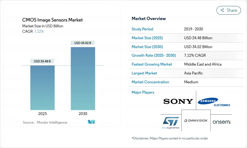
預計 CMOS 影像感測器市場規模將在 2025 年達到 245.8 億美元,到 2030 年將達到 345.2 億美元,複合年成長率為 7.12%。
從智慧型手機相機到汽車安全、工業自動化和醫療診斷,CMOS影像感測器的需求正在不斷擴大,這反映出該技術相對於CCD設計的功能優勢日益增強。採用片上AI邏輯的背照式(BSI)架構,在提升性能的同時降低了功耗,從而鞏固了CMOS影像感測器在大批量電子市場的成本領先地位。從區域來看,亞太地區是台灣代工廠的主要生產動力,而中東和非洲地區則在智慧城市監控部署的推動下實現了兩位數的成長。儘管美國和中國的出口限制以及300毫米晶圓的供不應求鏈風險,但行業整合仍在繼續,傳統製造商正在縮減產能並加速收購專業製造商。
全球CMOS影像感測器市場趨勢與洞察
亞太地區OEM廠商採用多鏡頭智慧型手機
亞太地區的行動電話廠商正將多攝影機陣列從旗艦機型擴展到中階機型,推動高動態範圍影像感測器的持續成長。三星計畫於2024年發表2億像素和5,000萬像素的ISOCELL感測器,凸顯了其對運算攝影和高影格速率影片的重視。 OmniVision的OV50X感光元件提供110dB的單次曝光HDR,顯示高階智慧型手機的差異化優勢不再僅僅體現在像素數量上,而是體現在感光元件效能上。SONY的LYT-828感測器預計將於2025年量產,其片上整合了混合幀HDR邏輯,無需外部ISP週期即可實現AI輔助的低照度處理。更高的像素密度和片上運算能力的結合,不僅支援了功能擴展,也推高了先進組件的平均售價,從而增強了CMOS影像感測器市場的收入成長。
美國和歐盟對ADAS攝影機的監管要求
美國國家公路交通安全管理局 (NHTSA) 將於 2024 年 12 月對其新車評估項目進行升級,屆時輕型車輛將強制要求配備基於攝影機的盲點監測、車道維持輔助和自動緊急煞車系統,這將推動對感測器的長期需求。全域百葉窗架構能夠減少運動偽影,這對安全關鍵型影像處理至關重要。斯巴魯的新一代 EyeSight 系統就充分體現了這一點,該系統採用了安森美半導體 (ON Semiconductor) 的 Hyperlux AR0823AT 感測器,符合 ASIL C 安全標準。歐盟的通用安全法規與美國的要求一致,規範同步,並為 CMOS 代工廠提供了長達十年的汽車級產能投資前景。
台灣及韓國300mm CIS晶圓產能限制現狀
對於台灣和韓國的代工廠而言,人工智慧晶片訂單正與影像感測器生產展開競爭,導致前置作業時間從12-16週延長至20-24週。儘管台積電在亞利桑那州的擴建項目投資了1,650億美元,但到2027年,該計畫不太可能大幅緩解獨立國協地區的產能瓶頸。堆疊式背照式晶片製造的地理集中加劇了地緣政治風險,顯著削弱了CMOS影像感測器市場近期的供應韌性。
細分市場分析
由於其卓越的靈敏度和高信噪比,背照式感測器預計在2024年將佔據CMOS影像感測器市場65%的佔有率。這一細分市場的崛起擴大了高階智慧型手機和車載攝影機等應用領域基於背照式(BSI)技術的CMOS影像感測器的市場規模。堆疊式BSI/3D感測器正以9.8%的複合年成長率快速發展,其整合的邏輯層可即時執行AI推理,進一步提升了每平方毫米感測器的價值。
前照式裝置在成本受限的產品系列(例如入門級物聯網相機)中仍將保持其重要性。全局百葉窗架構(通常基於流光溢流技術)將在工業自動化領域中得到更廣泛的應用,以消除運動偽影。預計在2026年至2030年間出現的新型玻璃基板3D堆疊技術可望實現更優異的散熱性能和更高的互連密度,從而擴大高階產品的差異化優勢。
到2024年,1,200萬至2,400萬像素頻寬將佔據CMOS影像感測器市場25%的佔有率,進而平衡主流行動裝置的儲存和運算開銷。 4,900萬像素及以上的設備雖然仍屬於小眾市場,但隨著監控、醫療和專業攝影領域對超高倍數位變焦的需求日益成長,其市場佔有率正以每年9.5%的速度攀升。Canon的4.1億像素原型機凸顯了全片幅超高密度感測器的技術可行性,並有望催生新的診斷成像模式。
像素低於 1,200 萬的感測器主要用於條碼掃描和行車記錄器等應用,在這些應用中,影格速率比清晰度更為重要。像素介於 2500 萬到 4800 萬之間的中端感測器則用於採用多幀計算疊加技術的無反光鏡相機。像素數量的這種差異加劇了 CMOS 影像感測器市場的價格細分,並維持了利潤率的差異。
區域分析
亞太地區將佔2024年全球營收的34%,並受惠於從晶圓代工到最終行動裝置組裝的垂直整合生態系統。台灣晶圓廠供應了大部分堆疊式背照式(BSI)晶圓,而中國當地仍然是全球最大的智慧型手機出口中心。以三星ISOCELL藍圖代表的韓國創新,使其在CMOS影像感測器市場保持技術領先地位。供應鏈集中化帶來了規模經濟效益,但也增加了地震和地緣政治風險。
到2030年,中東和非洲將以9.8%的複合年成長率實現最快成長,海灣地區的智慧城市規劃要求部署連網監視錄影機和交通分析攝影機。配備ADAS(高級駕駛輔助系統)的車輛進口將加快售後市場的更換週期,而非洲行動優先的電子商務蓬勃發展將推動低照度自拍攝影機的需求成長。公共和私人資金籌措獎勵將加速該地區的系統整合,為CMOS影像感測器市場的擴張開闢新的途徑。
北美正透過社群媒體平台的需求和嚴格的汽車安全法規影響全球設計。內容創作生態系統優先考慮針對高影格速率8K 影片拍攝最佳化的感測器,這促使本土無晶圓廠供應商進入高階細分市場。在德國工業 4.0 投資的推動下,歐洲正將光電研發轉向高可靠性的工業和醫療應用。南美和南亞市場尚未開發,但價格敏感度促使採購者傾向於成熟的中階設計,而非尖端感測器。
其他福利:
- Excel格式的市場預測(ME)表
- 3個月的分析師支持
目錄
第1章 引言
- 研究假設和市場定義
- 調查範圍
第2章調查方法
第3章執行摘要
第4章 市場情勢
- 市場概覽
- 市場促進因素
- 亞太地區OEM廠商對多鏡頭智慧型手機的採用情況
- 美國和歐盟對ADAS攝影機的監管要求
- 北美以影片為中心的社群媒體對4K/8K感測器的需求
- 日本和歐盟的穿戴式小型感測器用於醫療圖像診斷
- 中東智慧城市監控系統部署
- 德國工業4.0對工業自動化用全局百葉窗的需求
- 市場限制
- 台灣及韓國先進的300公厘CIS晶圓產能受限
- 入門級智慧型手機拉低了平均售價
- 高速攝影中的熱噪音和滾動百葉窗限制
- 美國和中國最先進的獨立國協出口管制措施
- 價值/供應鏈分析
- 監理與技術展望
- 波特五力分析
- 供應商的議價能力
- 買方的議價能力
- 新進入者的威脅
- 替代品的威脅
- 競爭對手之間的競爭
- 技術概覽(按通訊類型分類)
- 有線
- 無線的
- 投資分析
第5章 市場規模與成長預測
- 透過技術
- 前側照明(FSI)
- 背照式(BSI)
- 堆疊式BSI/3D
- 全域百葉窗CMOS
- 通過決議
- 低於1200萬像素
- 1200萬至2400萬像素
- 2500萬至4800萬像素
- 4900萬像素或以上
- 頻譜
- 可見頻譜
- 非可見光(近紅外線、紫外線、短波紅外線)頻譜
- 依通訊類型
- 有線
- 無線的
- 按最終用戶行業分類
- 消費性電子產品
- 汽車與運輸
- 工業和機器視覺
- 安全與監控
- 醫療保健和生命科學
- 計算和資料中心
- 航太/國防
- 按地區
- 北美洲
- 美國
- 加拿大
- 墨西哥
- 歐洲
- 英國
- 德國
- 法國
- 義大利
- 其他歐洲地區
- 亞太地區
- 中國
- 日本
- 印度
- 韓國
- 亞太其他地區
- 中東
- 以色列
- 沙烏地阿拉伯
- 阿拉伯聯合大公國
- 土耳其
- 其他中東地區
- 非洲
- 南非
- 埃及
- 其他非洲地區
- 南美洲
- 巴西
- 阿根廷
- 南美洲其他地區
- 北美洲
第6章 競爭情勢
- 策略趨勢
- 市佔率分析
- 公司簡介
- Sony Group Corporation
- Samsung Electronics Co., Ltd.
- OmniVision Technologies, Inc.
- onsemi Corporation
- STMicroelectronics NV
- Canon Inc.
- Panasonic Holdings Corporation
- SK Hynix Inc.
- Hamamatsu Photonics KK
- Teledyne Technologies Incorporated
- GalaxyCore Shanghai Limited Corporation
- SmartSens Technology Co., Ltd.
- PixArt Imaging Inc.
- Tower Semiconductor Ltd.
- ams-OSRAM AG
- Teledyne e2v(UK)Ltd.
- Himax Technologies, Inc.
- Siliconfile Technologies Inc.
- Sharp Corporation
- Caeleste CVBA
第7章 市場機會與未來展望
The CMOS image sensor market stands at USD 24.58 billion in 2025 and is forecast to reach USD 34.52 billion by 2030, registering a 7.12% CAGR.
Demand spreads from smartphone cameras to automotive safety, industrial automation and medical diagnostics, reflecting the technology's growing functionality advantages over CCD designs. Stacked backside-illuminated (BSI) architectures incorporating on-die AI logic raise performance while trimming power budgets, reinforcing the CMOS image sensor market's cost-leadership in mass-volume electronics. Regionally, Asia-Pacific anchors production through Taiwan's foundries, while Middle East and Africa outpace with double-digit expansion on smart-city surveillance deployments. Consolidation continues as legacy producers divest capacity and specialist acquisitions accelerate, even as U.S.-China export controls and 300 mm wafer shortages inject supply-chain risk.
Global CMOS Image Sensors Market Trends and Insights
Smartphone Multi-Camera Adoption by APAC OEMs
APAC handset makers are extending multi-camera arrays from flagships into mid-range lines, driving sustained unit growth for high-dynamic-range image sensors. Samsung's 2024 release of 200 MP and 50 MP ISOCELL devices underscored the pivot toward computational photography and higher frame-rate video. OmniVision's OV50X, offering 110 dB single-exposure HDR, illustrates how premium smartphones now differentiate on sensor capability rather than megapixel count alone. Sony's LYT-828, entering mass production in 2025, embeds Hybrid Frame-HDR logic on-die, allowing AI-assisted low-light processing without external ISP cycles. The combination of higher pixel densities and on-sensor compute supports feature expansion while raising average selling prices for advanced parts, reinforcing revenue growth for the CMOS image sensor market.
Regulatory Mandates for ADAS Cameras in US & EU
NHTSA's December 2024 New Car Assessment Program upgrade mandates camera-based blind-spot, lane-keeping and automatic emergency-braking systems across light vehicles, anchoring long-term sensor demand. Global-shutter architectures mitigate motion artifacts essential for safety-critical imaging, evident in Subaru's next-generation EyeSight system that selects onsemi's Hyperlux AR0823AT sensor meeting ASIL C safety standards. The EU's General Safety Regulation mirrors U.S. requirements, synchronizing specifications and giving CMOS foundry operators visibility for a decade of automotive-grade capacity investments.
Advanced 300 mm CIS Wafer Capacity Constraints in Taiwan & Korea
Surging AI-chip orders compete with image-sensor output for advanced 300 mm lines at Taiwanese and Korean foundries, extending lead times from 12-16 weeks to 20-24 weeks. TSMC's Arizona expansion, though capitalized at USD 165 billion, will not meaningfully relieve CIS bottlenecks before 2027. The geographic clustering of stacked BSI manufacturing heightens geopolitical exposure, significantly tempering near-term supply elasticity for the CMOS image sensor market.
Other drivers and restraints analyzed in the detailed report include:
- Video-Centric Social-Media Demand for 4K/8K Sensors in North America
- Miniaturized Sensors for Wearable Medical Imaging in Japan & EU
- ASP Erosion in Entry-Level Smartphones
For complete list of drivers and restraints, kindly check the Table Of Contents.
Segment Analysis
Backside-illuminated sensors captured 65% CMOS image sensor market share in 2024, reflecting superior sensitivity and higher signal-to-noise ratios. The segment's ascendancy lifted the BSI-based CMOS image sensor market size for premium smartphones and automotive cameras. Stacked BSI/3D sensors are advancing at 9.8% CAGR, integrating logic layers that execute AI inference in situ and further enlarge value per square millimeter.
Front-side-illuminated devices maintain relevance in cost-constrained SKUs such as entry-level IoT cameras. Global-shutter architectures, often FSI-based, gain adoption in industrial automation to thwart motion artefacts. Emerging glass-substrate 3D stacking, projected between 2026 and 2030, promises tighter thermal profiles and higher interconnect densities, widening high-end differentiation.
The 12-24 MP band accounted for 25% CMOS image sensor market share in 2024, balancing storage and compute overhead in mainstream handsets. >=49 MP devices, though niche, are growing 9.5% annually as surveillance, medical and professional photography favor extreme digital zoom. Canon's 410 MP prototype highlights technical viability of full-frame ultra-high-density sensors, potentially catalyzing new diagnostic imaging modalities.
Sub-12 MP parts endure in barcode scanning and dashcams where frame rate trumps definition. Mid-tier 25-48 MP sensors serve mirrorless cameras leveraging multi-frame computational overlays. The pixel-count bifurcation sharpens price segmentation across the CMOS image sensor market, preserving margin tiers.
The CMOS Image Sensor Market Report is Segmented by Technology (Front Side Illuminated, Backside-Illuminated, and More), Resolution ( Less Than 12 Megapixels, 12-24 Megapixels, and More ), Spectrum (Visible, Non-Visible), Communication Type (Wired, Wireless), End-User Industry (Consumer Electronics, Automotive, Industrial, and More), and Geography. The Market Forecasts are Provided in Terms of Value (USD).
Geography Analysis
Asia-Pacific holds 34% of 2024 revenue, benefiting from vertically integrated ecosystems spanning foundry silicon to final handset assembly. Taiwanese fabs supply the bulk of stacked-BSI wafers, while mainland China remains the world's largest smartphone export base. Korean innovation, led by Samsung's ISOCELL roadmap, sustains technology leadership inside the CMOS image sensor market. Supply-chain concentration confers scale economics yet elevates earthquake and geopolitical exposure.
Middle East and Africa present the fastest growth at 9.8% CAGR to 2030 as Gulf smart-city blueprints demand networked surveillance and traffic-analytics cameras. ADAS-equipped vehicle imports lift aftermarket replacement cycles, while Africa's mobile-first e-commerce boom drives low-light selfie camera volumes. Public-private funding incentives accelerate local system integration, creating an emerging corridor for CMOS image sensor market expansion.
North America influences global design through social-media platform demands and stringent automotive safety rules. Content-creator ecosystems prioritize sensors optimized for high-frame-rate 8K capture, pushing domestic fabless vendors toward premium niches. Europe, anchored by Germany's Industry 4.0 investments, channels photonics R&D into high-reliability industrial and medical segments. South America and South Asia represent untapped volume, though price sensitivity steers procurement toward established mid-tier designs rather than bleeding-edge sensors.
- Sony Group Corporation
- Samsung Electronics Co., Ltd.
- OmniVision Technologies, Inc.
- onsemi Corporation
- STMicroelectronics N.V.
- Canon Inc.
- Panasonic Holdings Corporation
- SK Hynix Inc.
- Hamamatsu Photonics K.K.
- Teledyne Technologies Incorporated
- GalaxyCore Shanghai Limited Corporation
- SmartSens Technology Co., Ltd.
- PixArt Imaging Inc.
- Tower Semiconductor Ltd.
- ams-OSRAM AG
- Teledyne e2v (UK) Ltd.
- Himax Technologies, Inc.
- Siliconfile Technologies Inc.
- Sharp Corporation
- Caeleste CVBA
Additional Benefits:
- The market estimate (ME) sheet in Excel format
- 3 months of analyst support
TABLE OF CONTENTS
1 INTRODUCTION
- 1.1 Study Assumptions and Market Definition
- 1.2 Scope of the Study
2 RESEARCH METHODOLOGY
3 EXECUTIVE SUMMARY
4 MARKET LANDSCAPE
- 4.1 Market Overview
- 4.2 Market Drivers
- 4.2.1 Smartphone Multi-Camera Adoption by APAC OEMs
- 4.2.2 Regulatory Mandates for ADAS Cameras in US and EU
- 4.2.3 Video-Centric Social Media Demand for 4K/8K Sensors in North America
- 4.2.4 Miniaturized Sensors for Wearable Medical Imaging in Japan and EU
- 4.2.5 Smart-City Surveillance Roll-outs in Middle East
- 4.2.6 Global-Shutter Demand for Industrial Automation in Germany's Industry 4.0
- 4.3 Market Restraints
- 4.3.1 Advanced 300-mm CIS Wafer Capacity Constraints in Taiwan and Korea
- 4.3.2 ASP Erosion in Entry-Level Smartphones
- 4.3.3 Thermal Noise and Rolling-Shutter Limits in High-Speed Cinematography
- 4.3.4 US-China Export Controls on Leading-Edge CIS
- 4.4 Value / Supply-Chain Analysis
- 4.5 Regulatory and Technological Outlook
- 4.6 Porter's Five Forces Analysis
- 4.6.1 Bargaining Power of Suppliers
- 4.6.2 Bargaining Power of Buyers
- 4.6.3 Threat of New Entrants
- 4.6.4 Threat of Substitutes
- 4.6.5 Intensity of Competitive Rivalry
- 4.7 Technology Snapshot (By Communication Type)
- 4.7.1 Wired
- 4.7.2 Wireless
- 4.8 Investment Analysis
5 MARKET SIZE AND GROWTH FORECASTS (VALUE)
- 5.1 By Technology
- 5.1.1 Front-Side Illuminated (FSI)
- 5.1.2 Backside-Illuminated (BSI)
- 5.1.3 Stacked BSI / 3-D
- 5.1.4 Global-Shutter CMOS
- 5.2 By Resolution
- 5.2.1 Less than 12 Megapixels
- 5.2.2 12-24 Megapixels
- 5.2.3 25-48 Megapixels
- 5.2.4 Greater than 49 Megapixels
- 5.3 By Spectrum
- 5.3.1 Visible Spectrum
- 5.3.2 Non-Visible (NIR, UV, SWIR) Spectrum
- 5.4 By Communication Type
- 5.4.1 Wired
- 5.4.2 Wireless
- 5.5 By End-user Industry
- 5.5.1 Consumer Electronics
- 5.5.2 Automotive and Transportation
- 5.5.3 Industrial and Machine Vision
- 5.5.4 Security and Surveillance
- 5.5.5 Healthcare and Life Sciences
- 5.5.6 Computing and Data-center
- 5.5.7 Aerospace and Defense
- 5.6 By Geography
- 5.6.1 North America
- 5.6.1.1 United States
- 5.6.1.2 Canada
- 5.6.1.3 Mexico
- 5.6.2 Europe
- 5.6.2.1 United Kingdom
- 5.6.2.2 Germany
- 5.6.2.3 France
- 5.6.2.4 Italy
- 5.6.2.5 Rest of Europe
- 5.6.3 Asia-Pacific
- 5.6.3.1 China
- 5.6.3.2 Japan
- 5.6.3.3 India
- 5.6.3.4 South Korea
- 5.6.3.5 Rest of Asia-Pacific
- 5.6.4 Middle East
- 5.6.4.1 Israel
- 5.6.4.2 Saudi Arabia
- 5.6.4.3 United Arab Emirates
- 5.6.4.4 Turkey
- 5.6.4.5 Rest of Middle East
- 5.6.5 Africa
- 5.6.5.1 South Africa
- 5.6.5.2 Egypt
- 5.6.5.3 Rest of Africa
- 5.6.6 South America
- 5.6.6.1 Brazil
- 5.6.6.2 Argentina
- 5.6.6.3 Rest of South America
- 5.6.1 North America
6 COMPETITIVE LANDSCAPE
- 6.1 Strategic Moves
- 6.2 Market Share Analysis
- 6.3 Company Profiles (includes Global level Overview, Market level overview, Core Segments, Financials as available, Strategic Information, Market Rank/Share for key companies, Products and Services, and Recent Developments)
- 6.3.1 Sony Group Corporation
- 6.3.2 Samsung Electronics Co., Ltd.
- 6.3.3 OmniVision Technologies, Inc.
- 6.3.4 onsemi Corporation
- 6.3.5 STMicroelectronics N.V.
- 6.3.6 Canon Inc.
- 6.3.7 Panasonic Holdings Corporation
- 6.3.8 SK Hynix Inc.
- 6.3.9 Hamamatsu Photonics K.K.
- 6.3.10 Teledyne Technologies Incorporated
- 6.3.11 GalaxyCore Shanghai Limited Corporation
- 6.3.12 SmartSens Technology Co., Ltd.
- 6.3.13 PixArt Imaging Inc.
- 6.3.14 Tower Semiconductor Ltd.
- 6.3.15 ams-OSRAM AG
- 6.3.16 Teledyne e2v (UK) Ltd.
- 6.3.17 Himax Technologies, Inc.
- 6.3.18 Siliconfile Technologies Inc.
- 6.3.19 Sharp Corporation
- 6.3.20 Caeleste CVBA
7 MARKET OPPORTUNITIES AND FUTURE OUTLOOK
- 7.1 White-Space and Unmet-Need Assessment
 CMOS影像感測器市場預測至2032年:按類型、頻譜、解析度、影像處理技術、最終用戶和地區分類的分析
 CMOS相機模組市場(按應用、產品類型、最終用戶、介面類型和解析度)—全球預測 2025-2032
 2025-2029年全球製藥業CMO市場
 2025-2029年全球CMOS相機模組市場
 有機 CMOS 影像感測器市場規模、佔有率、成長分析,按影像處理、按陣列類型、按應用、按行業部門、按地區 - 產業預測,2025 年至 2032 年
 全球 CMOS 影像感測器市場:市場規模、市場佔有率和趨勢分析(按頻譜、影像處理技術、解析度、最終用途和地區)、按細分市場預測(2025-2030 年)
 CMOS SCMOS 影像感測器市場 - 全球產業規模、佔有率、趨勢、機會和預測,按技術、規格、晶圓尺寸、感測器尺寸、應用、地區和競爭細分,2019-2029F
 CMOS影像感測器的全球市場:洞察·預測 (~2030年)全球 CMOS 影像感測器市場:按類型、應用和最終用戶產業分類 - 預測 2024-2030 年