


 |
市場調查報告書
商品編碼
1851511
覆晶技術:市場佔有率分析、行業趨勢、統計數據和成長預測(2025-2030 年)Flip Chip Technology - Market Share Analysis, Industry Trends & Statistics, Growth Forecasts (2025 - 2030) |
||||||
※ 本網頁內容可能與最新版本有所差異。詳細情況請與我們聯繫。
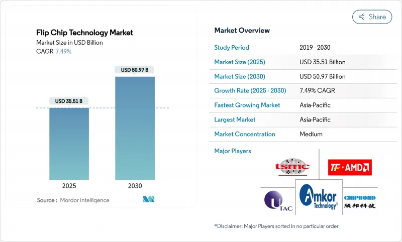
預計到 2025 年,覆晶技術市場規模將達到 355.1 億美元,到 2030 年將達到 509.7 億美元,年複合成長率為 7.49%。
這一成長反映了半導體產業向晶片級架構的轉型,這種架構需要高密度、散熱效率高的互連技術。人工智慧資料中心的建設推動了高頻寬記憶體封裝技術的發展,銅柱和混合鍵合線滿足了傳統焊料凸塊無法滿足的細間距需求。代工廠紛紛進軍封裝領域,加速了垂直整合,並對外包組裝和測試服務商構成了新的競爭壓力。儘管亞太地區保持了規模優勢,但北美和歐洲的供應鏈風險緩解計畫促使當地對先進封裝設施進行了大量待開發區投資。
全球覆晶技術市場趨勢與洞察
對異質整合(人工智慧/高效能運算)的需求快速成長
晶片製造商已從2D微縮轉向異構整合,將多個晶片封裝在單一封裝上,從而推動了對細間距銅-銅互連的需求。台積電計畫在2026年將CoWoS產能提升至131萬片,顯示英偉達等GPU廠商如何塑造了覆晶技術市場。與傳統的凸塊封裝技術相比,這種方法在提高頻寬的同時降低了功耗,從而支援了人工智慧加速器的效能藍圖。
銅柱凸塊和微凸塊互連技術的日益普及
銅柱凸塊具有優異的電阻和可靠性,預計在2024年將佔據46.3%的市佔率。杜邦公司的高速電鍍技術實現了均勻的厚度控制,這對於間距小於40µm的晶片至關重要。這一轉變削弱了錫鉛晶片的主導地位,並為支援覆晶技術市場的3D整合方案鋪平了道路。
先進凸塊生產線資本密集度高
將間距縮小到10微米以下需要光刻步進機、先進的濺射設備和等離子清洗機,導致每模組生產線成本超過2.5億美元。台積電在專用封裝廠投資900億美元,凸顯了小型競爭對手進入該領域的高門檻。聯合研發項目,例如3M參與的美國JOINT聯盟,旨在分散整個供應鏈的風險。
細分市場分析
覆晶覆晶技術市場規模預計將以9.8%的複合年成長率成長。這種混合鍵合方式已將晶片間距縮小至0.8µm,遠超焊料的物理極限。錫鉛解決方案仍適用於傳統製程節點,而金凸塊技術仍主要應用於航太領域。
電鍍化學技術的進步使柱體高度均勻性保持在2%以內,這是實現3D堆疊的先決條件。 IEEE的研究表明,在260°C下進行無焊料銅-銅鍵合是一種可行的異質整合製造方法。技術創新使得銅基材料能夠從無鉛和貴金屬替代品中奪取市場佔有率。
FC-BGA封裝憑藉其在伺服器領域久經考驗的可靠性,預計到2024年將佔總收入的38.1%。扇出型WLP和麵板級封裝預計將達到10.1%的複合年成長率,這主要得益於AI加速器對更大尺寸封裝體的需求。日月光(ASE)已撥款2億美元用於310mm x 310mm面板封裝,該封裝可提供七倍於傳統晶圓的可用面積。隨著產量比率線良率的提高,面板級封裝中覆晶技術的市場規模也將隨之擴大。
CoWoS 和 EMIB 等專用藍圖實現了 HBM 堆疊,這對 AI 訓練單元至關重要。 IBM 和英特爾致力於研發玻璃基板,與有機層壓板相比,玻璃基板具有更低的翹曲度和更高的線間距比。由於高成本且製程複雜,採用 TSV 技術的 3D IC 在超高頻寬元件領域仍處於小眾應用,但它們也限制了可實現的效能上限。
覆晶技術市場按晶圓凸塊製程(銅柱、錫鉛共晶焊料等)、封裝技術(FC-BGA、FCCSP/CSP等)、產品(記憶體、CMOS影像感測器等)、終端用戶產業(消費性電子和穿戴式設備、汽車和運輸、工業和機器人等)以及地區(北美、南美、歐洲、亞太地區細分、中東和機器人等)以及地區(北美、南美、歐洲、亞太地區細分、中東和機器人等)以及地區(北美、南美、歐洲、亞太地區、中東和機器人)進行細分。
區域分析
亞太地區預計到2024年將佔總收入的54.5%。該地區擁有絕大多數晶圓廠,並保持著成本優勢,因此在覆晶技術市場佔據最大佔有率。政府激勵措施支持了下一代晶片的研發,但出口限制促使主要公司在海外建立並行產能。在北美,《晶片法案》(CHIPS Act)加速了晶圓代工和封裝產推出的提升,增強了市場韌性並推動了本地需求。隨著亞利桑那州和德克薩斯州的園區投入營運,預計北美覆晶技術市場佔有率將小幅成長。
歐洲透過《歐洲晶片法案》追求技術主權,並將資金投入面板級和玻璃芯基板生產線。 Silicon Box位於諾瓦拉的工廠預計到2028年每周可加工1萬塊面板,為該地區的生態系統提供支援。中東和非洲仍處於起步階段,但受益於電子產品最終組裝中心對全球供應鏈的貢獻。
供應鏈多元化將使未來的投資分散到至少三大洲,削弱任何單一地區的統治地位,但亞太地區仍然擁有無與倫比的工程技術深度,並且仍然是大規模製造的中心。
其他福利:
- Excel格式的市場預測(ME)表
- 3個月的分析師支持
目錄
第1章 引言
- 研究假設和市場定義
- 調查範圍
第2章調查方法
第3章執行摘要
第4章 市場情勢
- 市場概覽
- 市場促進因素
- 對異質整合(人工智慧/高效能運算)的需求快速成長
- 銅柱和微凸塊互連技術的日益普及
- 穿戴式裝置和物聯網領域小型化趨勢
- 汽車ADAS/電動車的可靠性要求
- 玻璃芯基板的商業測試
- 對晶片級銅-銅混合鍵結的需求
- 市場限制
- 先進凸塊生產線資本密集度高
- 無鉛可靠度與翹曲挑戰
- 對準產量比率損失小於 10 μm
- 關鍵金屬化學品供應鏈
- 價值鏈分析
- 宏觀經濟因素的影響
- 監管環境
- 技術展望
- 波特五力模型
- 供應商的議價能力
- 買方的議價能力
- 新進入者的威脅
- 替代品的威脅
- 競爭對手之間的競爭
- 投資分析
第5章 市場規模與成長預測
- 透過晶圓凸塊工藝
- 銅柱
- 錫鉛共晶焊料
- 無鉛焊料(錫銀焊料、SAC焊料等)
- 金耳環碰撞
- 銅/銅混合/直接鍵合
- 透過包裝技術
- FC-BGA(2D/2.1D/2.5D/3D)
- FCCSP/CSP
- CoWoS/InFO/EMIB
- 扇出 WLP/PLP
- 採用TSV的3D積體電路
- 依產品
- 記憶體(DRAM、HBM)
- CMOS影像感測器
- LED 和迷你/微型 LED
- SoC/應用處理器
- GPU/AI加速器
- CPU/伺服器處理器
- 按最終用途行業分類
- 消費性電子產品和穿戴式裝置
- 汽車與運輸
- 工業機器人
- 通訊和5G基礎設施
- 資料中心和雲
- 軍事/航太
- 醫療和保健設備
- 按地區
- 北美洲
- 美國
- 加拿大
- 墨西哥
- 南美洲
- 巴西
- 其他南美洲
- 歐洲
- 德國
- 法國
- 英國
- 俄羅斯
- 其他歐洲地區
- 亞太地區
- 中國
- 台灣
- 韓國
- 日本
- 馬來西亞
- 新加坡
- 亞太其他地區
- 中東和非洲
- 中東
- 土耳其
- 其他中東地區
- 非洲
- 南非
- 其他非洲地區
- 北美洲
第6章 競爭情勢
- 市場集中度
- 策略性舉措(併購、合資、產能擴張)
- 市佔率分析
- 公司簡介
- Amkor Technology, Inc.
- ASE Technology Holding Co., Ltd.
- Taiwan Semiconductor Manufacturing Company Limited
- Jiangsu Changjiang Electronics Technology Co., Ltd.
- Powertech Technology Inc.
- Chipbond Technology Corporation
- UTAC Holdings Ltd.
- TF-AMD Microelectronics Sdn. Bhd.
- Shinko Electric Industries Co., Ltd.
- Unisem(M)Berhad
- Hana Micron Inc.
- Nepes Corporation
- Carsem(M)Sdn. Bhd.
- Sigurd Microelectronics Corporation
- AT&S Austria Technologie & Systemtechnik AG
- Intel Corporation
- Samsung Electronics Co., Ltd.
- Advanced Micro Devices, Inc.
- Texas Instruments Incorporated
- United Microelectronics Corporation
- STATS ChipPAC Pte. Ltd.
- SFA Semicon Co., Ltd.
- Tongfu Microelectronics Co., Ltd.
- Huatian Technology Co., Ltd.
- Lingsen Precision Industries, Ltd.
第7章 市場機會與未來展望
The flip chip technology market size stood at USD 35.51 billion in 2025 and is on track to reach USD 50.97 billion by 2030, reflecting a 7.49% CAGR.
Growth mirrored the semiconductor industry's transition to chiplet-based architectures that required dense, thermally efficient interconnects. AI data-center build-outs pushed high-bandwidth memory packaging to the fore, while copper-pillar and hybrid bonding lines addressed the fine-pitch needs that traditional solder bumps could not meet. Foundries entered the packaging arena, accelerating vertical integration and bringing new competitive pressures on outsourced assembly and test providers. Asia-Pacific retained scale advantages, yet supply-chain de-risking programs in North America and Europe triggered large green-field investments in advanced packaging facilities.
Global Flip Chip Technology Market Trends and Insights
Surge in Heterogeneous Integration Demand (AI/HPC)
Chipmakers pivoted from 2D scaling to heterogeneous integration that joined multiple chiplets in a single package, lifting demand for fine-pitch Cu-to-Cu interconnects. TSMC's plan to boost CoWoS capacity to 1.31 million units by 2026 illustrated how GPU vendors such as Nvidia shaped the flip chip technology market. The approach enhanced bandwidth while lowering power compared with legacy bumps, supporting the performance roadmap for AI accelerators.
Rising Adoption of Copper-Pillar and Micro-Bump Interconnects
Copper-pillar bumps delivered superior electrical resistance and reliability, explaining their 46.3% 2024 revenue share. High-speed plating chemistries from DuPont provided uniform thickness control essential for sub-40 µm pitches. The shift eroded tin-lead dominance and paved the way for 3D integration schemes that underpin the flip chip technology market.
High Capital Intensity of Advanced Bumping Lines
Scaling to sub-10 µm pitches required lithography steppers, advanced sputter tools, and plasma cleaners that pushed line cost above USD 250 million per module. TSMC earmarked USD 90 billion for dedicated packaging plants, underscoring the entry hurdle for smaller competitors. Collaborative R&D programs such as 3M's participation in the US-JOINT consortium aimed to spread risk across the supply chain.
Other drivers and restraints analyzed in the detailed report include:
- Wearables and IoT Miniaturization Push
- Automotive ADAS/EV Reliability Requirements
- Lead-Free Reliability and Warpage Challenges
For complete list of drivers and restraints, kindly check the Table Of Contents.
Segment Analysis
Copper pillar technology held 46.3% revenue in 2024 within the flip chip technology market. The segment benefited from reduced resistance and heightened current-carrying capability. The flip chip technology market size for Cu-to-Cu hybrid bonding is projected to expand at a 9.8% CAGR as chiplet adoption grows. The hybrid method lowered inter-chip spacing to 0.8 µm, far beyond solder's physical limits. Tin-lead solutions still served legacy nodes, whereas gold-stud bumps remained confined to aerospace.
Advances in electroplated chemistries sustained pillar height uniformity below 2%, a prerequisite for 3D stacks. IEEE research validated solder-free Cu-Cu bonding at 260 °C as a manufacturable path for heterogeneous integration. Innovations positioned copper formats to absorb share from both lead-free and precious-metal alternatives.
FC-BGA commanded 38.1% of 2024 revenue thanks to proven reliability in servers. Fan-out WLP and panel-level formats are expected to record a 10.1% CAGR, catalyzed by AI accelerators demanding large body sizes. ASE allocated USD 200 million to 310 mm X 310 mm panels that promise sevenfold usable area over wafers, a cost breakthrough. The flip chip technology market size for panel-level packages will climb as line yields improve.
Specialty flows such as CoWoS and EMIB enable HBM stacking essential for AI training units. IBM and Intel pursued glass-substrate roadmaps that offer lower warpage and higher line-space ratios than organic laminates. 3D IC with TSV remained a niche for extreme bandwidth-class devices due to high cost and process complexity, but set the ceiling on attainable performance.
Flip Chip Technology Market is Segmented by Wafer Bumping Process (Copper Pillar, Tin-Lead Eutectic Solder, and More), Packaging Technology (FC-BGA, FCCSP/CSP, and More), Product (Memory, CMOS Image Sensor, and More), End-Use Industry (Consumer Electronics and Wearables, Automotive and Transportation, Industrial and Robotics, and More), and Geography (North America, South America, Europe, Asia-Pacific, and Middle East and Africa).
Geography Analysis
Asia-Pacific held 54.5% of 2024 revenue. The region housed the bulk of wafer fabs and retained cost advantages, sustaining the largest slice of the flip chip technology market. Government incentives supported next-node R&D, yet export-control actions induced leading firms to build parallel capacity offshore. North America accelerated foundry and packaging startups under the CHIPS Act, adding resilience and creating a local demand pull. The flip chip technology market share for North America is expected to rise modestly as Arizona and Texas campuses come online.
Europe pursued technology sovereignty through the European Chips Act and directed capital toward panel-level and glass-core substrate lines. Silicon Box's Novara facility is slated to process 10,000 panels weekly by 2028, anchoring a regional ecosystem. Middle East and Africa remained early-stage but benefited from electronics final-assembly hubs that feed into global supply chains.
Supply-chain diversification scattered future investments across at least three continents, muting single-region dominance. However, Asia-Pacific still boasted unmatched engineering depth, keeping it the reference center for high-volume manufacturing.
- Amkor Technology, Inc.
- ASE Technology Holding Co., Ltd.
- Taiwan Semiconductor Manufacturing Company Limited
- Jiangsu Changjiang Electronics Technology Co., Ltd.
- Powertech Technology Inc.
- Chipbond Technology Corporation
- UTAC Holdings Ltd.
- TF-AMD Microelectronics Sdn. Bhd.
- Shinko Electric Industries Co., Ltd.
- Unisem (M) Berhad
- Hana Micron Inc.
- Nepes Corporation
- Carsem (M) Sdn. Bhd.
- Sigurd Microelectronics Corporation
- AT&S Austria Technologie & Systemtechnik AG
- Intel Corporation
- Samsung Electronics Co., Ltd.
- Advanced Micro Devices, Inc.
- Texas Instruments Incorporated
- United Microelectronics Corporation
- STATS ChipPAC Pte. Ltd.
- SFA Semicon Co., Ltd.
- Tongfu Microelectronics Co., Ltd.
- Huatian Technology Co., Ltd.
- Lingsen Precision Industries, Ltd.
Additional Benefits:
- The market estimate (ME) sheet in Excel format
- 3 months of analyst support
TABLE OF CONTENTS
1 INTRODUCTION
- 1.1 Study Assumptions and Market Definition
- 1.2 Scope of the Study
2 RESEARCH METHODOLOGY
3 EXECUTIVE SUMMARY
4 MARKET LANDSCAPE
- 4.1 Market Overview
- 4.2 Market Drivers
- 4.2.1 Surge in heterogeneous integration demand (AI/ HPC)
- 4.2.2 Rising adoption of copper-pillar and micro-bump interconnects
- 4.2.3 Wearables and IoT miniaturization push
- 4.2.4 Automotive ADAS/EV reliability requirements
- 4.2.5 Glass-core substrate commercial trials
- 4.2.6 Demand for chip-let-ready Cu-to-Cu hybrid bonding
- 4.3 Market Restraints
- 4.3.1 High capital intensity of advanced bumping lines
- 4.3.2 Lead-free reliability and warpage challenges
- 4.3.3 Sub-10 µm alignment yield losses
- 4.3.4 Supply-chain exposure to critical metal chemicals
- 4.4 Value Chain Analysis
- 4.5 Impact of Macroeconomic Factors
- 4.6 Regulatory Landscape
- 4.7 Technological Outlook
- 4.8 Porter's Five Forces
- 4.8.1 Bargaining Power of Suppliers
- 4.8.2 Bargaining Power of Buyers
- 4.8.3 Threat of New Entrants
- 4.8.4 Threat of Substitutes
- 4.8.5 Intensity of Competitive Rivalry
- 4.9 Investment Analysis
5 MARKET SIZE AND GROWTH FORECASTS (VALUE)
- 5.1 By Wafer Bumping Process
- 5.1.1 Copper Pillar
- 5.1.2 Tin-Lead Eutectic Solder
- 5.1.3 Lead-Free Solder (SnAg, SAC, etc.)
- 5.1.4 Gold-Stud Bumping
- 5.1.5 Cu-to-Cu Hybrid / Direct Bond
- 5.2 By Packaging Technology
- 5.2.1 FC-BGA (2D/2.1D/2.5D/3D)
- 5.2.2 FCCSP / CSP
- 5.2.3 CoWoS / InFO / EMIB
- 5.2.4 Fan-Out WLP / PLP
- 5.2.5 3D IC with TSV
- 5.3 By Product
- 5.3.1 Memory (DRAM, HBM)
- 5.3.2 CMOS Image Sensor
- 5.3.3 LED and Mini/Micro-LED
- 5.3.4 SoC / Application Processor
- 5.3.5 GPU / AI Accelerator
- 5.3.6 CPU / Server Processor
- 5.4 By End-Use Industry
- 5.4.1 Consumer Electronics and Wearables
- 5.4.2 Automotive and Transportation
- 5.4.3 Industrial and Robotics
- 5.4.4 Telecommunications and 5G Infrastructure
- 5.4.5 Data Center and Cloud
- 5.4.6 Military and Aerospace
- 5.4.7 Medical and Healthcare Devices
- 5.5 By Geography
- 5.5.1 North America
- 5.5.1.1 United States
- 5.5.1.2 Canada
- 5.5.1.3 Mexico
- 5.5.2 South America
- 5.5.2.1 Brazil
- 5.5.2.2 Rest of South America
- 5.5.3 Europe
- 5.5.3.1 Germany
- 5.5.3.2 France
- 5.5.3.3 United Kingdom
- 5.5.3.4 Russia
- 5.5.3.5 Rest of Europe
- 5.5.4 Asia-Pacific
- 5.5.4.1 China
- 5.5.4.2 Taiwan
- 5.5.4.3 South Korea
- 5.5.4.4 Japan
- 5.5.4.5 Malaysia
- 5.5.4.6 Singapore
- 5.5.4.7 Rest of Asia-Pacific
- 5.5.5 Middle East and Africa
- 5.5.5.1 Middle East
- 5.5.5.1.1 Turkey
- 5.5.5.1.2 Rest of Middle East
- 5.5.5.2 Africa
- 5.5.5.2.1 South Africa
- 5.5.5.2.2 Rest of Africa
- 5.5.1 North America
6 COMPETITIVE LANDSCAPE
- 6.1 Market Concentration
- 6.2 Strategic Moves (M&A, JV, Capacity Expansions)
- 6.3 Market Share Analysis
- 6.4 Company Profiles (includes Global-level Overview, Market-level Overview, Core Segments, Financials, Strategic Information, Market Rank/Share, Products and Services, Recent Developments)
- 6.4.1 Amkor Technology, Inc.
- 6.4.2 ASE Technology Holding Co., Ltd.
- 6.4.3 Taiwan Semiconductor Manufacturing Company Limited
- 6.4.4 Jiangsu Changjiang Electronics Technology Co., Ltd.
- 6.4.5 Powertech Technology Inc.
- 6.4.6 Chipbond Technology Corporation
- 6.4.7 UTAC Holdings Ltd.
- 6.4.8 TF-AMD Microelectronics Sdn. Bhd.
- 6.4.9 Shinko Electric Industries Co., Ltd.
- 6.4.10 Unisem (M) Berhad
- 6.4.11 Hana Micron Inc.
- 6.4.12 Nepes Corporation
- 6.4.13 Carsem (M) Sdn. Bhd.
- 6.4.14 Sigurd Microelectronics Corporation
- 6.4.15 AT&S Austria Technologie & Systemtechnik AG
- 6.4.16 Intel Corporation
- 6.4.17 Samsung Electronics Co., Ltd.
- 6.4.18 Advanced Micro Devices, Inc.
- 6.4.19 Texas Instruments Incorporated
- 6.4.20 United Microelectronics Corporation
- 6.4.21 STATS ChipPAC Pte. Ltd.
- 6.4.22 SFA Semicon Co., Ltd.
- 6.4.23 Tongfu Microelectronics Co., Ltd.
- 6.4.24 Huatian Technology Co., Ltd.
- 6.4.25 Lingsen Precision Industries, Ltd.
7 MARKET OPPORTUNITIES AND FUTURE OUTLOOK
- 7.1 White-space and Unmet-Need Assessment
 倒裝晶片/WLP製造與市場分析
 覆晶封裝市場:依封裝類型、封裝格式、技術節點、組裝流程、終端用戶產業及應用分類-2026-2032年全球市場預測覆晶技術市場:2026-2032年全球市場預測(依安裝類型、封裝、凸塊材料、晶圓尺寸、應用及最終用戶產業分類)覆晶市場:依封裝技術、凸塊技術、晶圓尺寸、組裝類型、焊料凸塊類型、基板材料、應用、終端用戶產業分類,全球預測,2026-2032年
 全球覆晶市場:依凸塊類型、封裝技術、終端應用產業、國家及地區分類-產業分析、市場規模、佔有率及預測(2025-2032年)
 覆晶市場分析及預測(至2035年):依類型、產品類型、服務、技術、組件、應用、材料類型、製程、最終用戶、設備分類
 全球覆晶市場規模、佔有率、趨勢和成長分析報告(2026-2034)
 2026年全球覆晶市場報告倒裝晶片市場規模、佔有率、成長及全球產業分析:依類型、應用和地區劃分的洞察與預測(2026-2034)覆晶BGA市場按產品類型、焊球數量、基板材料、裝置類型、分銷管道和應用分類-2026-2032年全球預測