


 |
市場調查報告書
商品編碼
2066536
類PCB基板:市場佔有率分析、產業趨勢與統計及成長預測(2026-2031年)Substrate-Like Printed Circuit Board - Market Share Analysis, Industry Trends & Statistics, Growth Forecasts (2026 - 2031) |
||||||
※ 本網頁內容可能與最新版本有所差異。詳細情況請與我們聯繫。
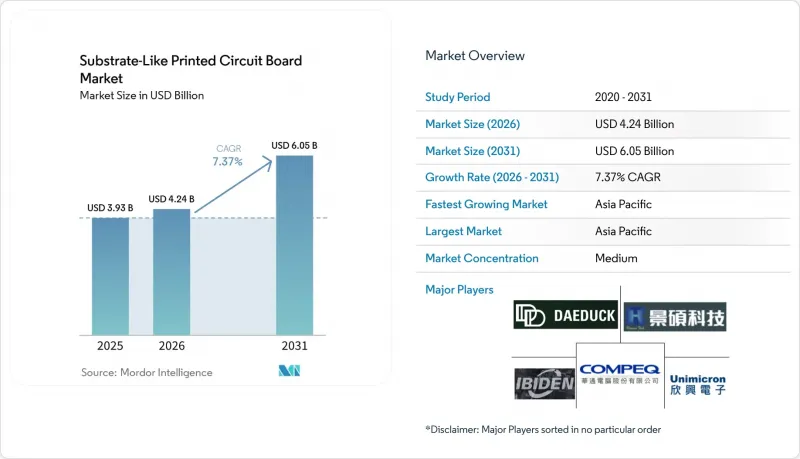
據 Mordor Intelligence 稱, 基板類設計的市場規模預計在 2026 年達到 42.4 億美元,高於 2025 年的 39.3 億美元,預計從 2026 年到 2031 年將達到 60.5 億美元,複合年成長率為 7.37%。
本報告按基板(玻璃纖維環氧樹脂FR-4、高速/低損耗、聚醯亞胺等)、終端用戶產業(家用電子電器、運算和資料中心、通訊和5G、汽車和電動車、醫療保健/醫療、航太和國防等)以及地區(北美、歐洲等)進行細分。市場預測以美元(USD)為單位。
全球類基板市場趨勢與洞察
智慧型手機OEM廠商對高密度互連的需求激增
智慧型手機製造商正將應用處理器、射頻前端和電源管理積體電路整合到基板印刷電路板 (SLP) 上,與傳統的多層設計相比,面積減少了 30%。根據台灣製造商預測,到 2025 年,行動應用預計將佔 SLP 銷售額的 35% 以上,這凸顯了對通孔直徑小於 50µm 和小於 20µm 的線路日益成長的需求。隨著越來越多的工廠掌握了這些微結構的製造技術,良率正成為關鍵的差異化因素,迫使供應商將高精度雷射直接曝光技術與預測分析相結合,以便及早發現圖案轉移偏差。
對5G通訊模組的需求不斷成長
運行於毫米波頻段的獨立組網(SA)5G網路在30 GHz頻率下插入損耗限制為0.5 dB-in,但FR-4基板在實際厚度下無法滿足此要求。因此,基地台OEM廠商開始採用高速PTFE或液晶聚合物層壓基板,其層數超過八層,從而推動了基板型PCB(SLP)市場的資本投入,用於自動化光學檢測(AOI),以將缺陷率控制在50 PPM以下。行動電話製造商也呈現類似的趨勢,雙頻終端在高密度SLP模組上整合了多個功率放大器和天線調諧器,從而提升了單一設備的材料銷售量。
SLP生產線的高額資本投入
一座能夠處理25微米線寬的新工廠需要1.5億至3億美元,用於實施雷射直接曝光、順序層壓和線上X光檢測叢集。由於除非運轉率超過80%,否則需要五年以上的時間才能收回投資,這阻礙了新進入者,並重塑了PCB市場格局。目前,PCB市場由現有企業主導,這些企業透過與通訊、基板電子和汽車行業的公司簽訂合約來攤銷資產。
細分市場分析
預計到2025年,高速低損耗層壓板將佔基板PCB市場40.94%的佔有率,並將在2031年之前以7.64%的複合年成長率成長。這是因為聚四氟乙烯(PTFE)、液晶聚合物和碳氫化合物陶瓷材料將取代玻璃環氧樹脂,用於5G無線網卡和400GbE交換結構。即使佈線長度更短,10GHz頻率下的插入損耗也能維持在0.5dB以下,進而提高頻譜效率,直接提升載波容量。玻璃環氧樹脂FR-4在中階智慧型手機和工業控制設備中仍佔據主導地位,因為其原料成本僅為PTFE複合材料的三分之一。然而,隨著行動電話製造商對堆疊式相機陣列的精度要求越來越高,FR-4在基板PCB市場的佔有率正開始萎縮。
高速材料在資料中心加速器電路板中也日益普及,其中112 Gbps PAM4訊號傳輸提高了眼圖閉合靈敏度。供應商開始將碳氫化合物陶瓷摻入ABF樹脂中,以提高玻璃化轉變溫度而不犧牲介電常數。聚醯亞胺在汽車和航空電子的軟性-剛性結構中佔有一席之地,但由於雷射鑽孔時間和化學品處理等製程成本較高,其市佔率仍低於10%。當熱通量超過10 W cm⁻²時,插座級功率電子領域會採用金屬芯和陶瓷填充結構。這是一個利潤率高但產量有限的微型細分市場。
區域分析
預計到2025年,亞太地區將佔基板類PCB市場銷售額的83.64%,主要驅動力來自台灣、中國大陸、韓國和日本。台灣在2024年第三季錄得205億美元的PCB產值,這反映出其擁有一個由疊層板供應商、雷射設備製造商和能夠在數日內完成原型製作的設計公司組成的生態系統。中國當地正在擴大國內產能,以減少對地緣政治不穩定的進口產品的依賴,例如,深南電路(Shennan Circuits)在政府補貼(SCC)的幫助下擴大了其ABF生產線。韓國企業集團正利用其在汽車行業的認證垂直整合業務進軍電動車模組市場,而日本則繼續保持其在超薄玻璃芯製程技術領域的領先地位。在5G普及、雲端資料中心建置和電動車電池組在地化生產的推動下,預計到2031年,全部區域將成長8.77%。
即使將北美和歐洲的市佔率加起來,仍低於15%,高昂的人事費用和薄弱的材料供應鏈是阻礙因素。儘管2022年的《晶片與科學法案》為半導體產業撥款390億美元,但由於基板製造設施被排除在投資稅額扣抵之外,短期內製造業回流的勢頭有所放緩。截至2026年初,紐約和奧地利等地的幾個待開發區先導計畫仍處於位置階段。世界其他地區的需求主要來自東南亞的消費性電子產品最終組裝和墨西哥的汽車線束工廠,但當地的基板產能有限,因此主要依賴從台灣和韓國進口。
地緣政治風險正促使跨國汽車製造商轉向雙重採購。優尼美光(Unimicron)位於泰國的工廠將於2025年開始量產,將使其產品免關稅進入東協市場,同時降低對台灣海峽風險的依賴。由於擔心台灣地震可能導致供應中斷,歐洲汽車製造商已與韓國和日本的供應商簽署了多年採購協議,以確保800V電池組基板類PCB(SLPCB)市場的持續供應。
其他好處:
- Excel格式的市場預測(ME)表
- 3個月的分析師支持
目錄
第1章:引言
- 研究假設和市場定義
- 調查範圍
第2章:調查方法
第3章執行摘要
第4章 市場狀況
- 市場概覽
- 市場促進因素
- 光學整合中超薄玻璃芯的應用
- 裝置內產生的 AI 正在增加 SLP 中的層數。
- 封裝內射頻前端整合(SiP + SLP)
- 採用能源採集SLP板的無電池穿戴裝置。
- 政府對先進基板晶片的津貼
- 越南積層製造膜產能迅速擴張
- 市場限制因素
- ABF樹脂市場的寡占狀態導致價格波動。
- 由於mSAP銅過度蝕刻導致材料尺寸小於20µm時良率降低。
- 熟練的mSAP流程工程師短缺
- 高能量等離子體去除術的碳足跡法規
- 宏觀經濟因素對市場的影響
- 產業價值鏈分析
- 監理情勢
- 技術展望
- 波特五力分析
第5章 市場規模與成長預測
- 按基板
- 玻璃環氧樹脂(FR-4)
- 高速/低損耗
- 聚醯亞胺(PI)
- 其他基板
- 按最終用戶行業分類
- 家用電子產品
- 計算和資料中心
- 通訊和5G
- 汽車和電動車
- 醫療保健/醫療
- 航太/國防
- 其他終端用戶產業
- 按地區
- 北美洲
- 美國
- 其他北美國家
- 歐洲
- 德國
- 英國
- 荷蘭
- 其他歐洲國家
- 亞太地區
- 中國
- 台灣
- 日本
- 印度
- 韓國
- 東南亞
- 其他亞太國家
- 世界其他地區
- 北美洲
第6章 競爭情勢
- 市場集中度
- 策略趨勢
- 市佔率分析
- 公司簡介
- Kinsus Interconnect Technology Corp
- Ibiden Co., Ltd.
- Compeq Manufacturing Co., Ltd.
- Daeduck Electronics Co., Ltd.
- Unimicron Technology Corp.
- Zhen Ding Technology Holding
- TTM Technologies
- Meiko Electronics Co., Ltd.
- AT&S AG
- Korea Circuit Co., Ltd.
- LG Innotek Co., Ltd.
- Samsung Electro-Mechanics
- Shennan Circuits Co., Ltd.
- Tripod Technology
- Fujitsu Interconnect
- Wus Printed Circuit
- HannStar Board Corp.
- Nippon Mektron Ltd.
- NCAB Group AB
第7章 市場機會與未來展望
According to Mordor Intelligence, the substrate-Like printed circuit board market size in 2026 is estimated at USD 4.24 billion, growing from 2025 value of USD 3.93 billion with projections showing USD 6.05 billion, growing at 7.37% CAGR over 2026-2031.
This report is Segmented by Substrate Material (Glass Epoxy FR-4, High-Speed/Low-Loss, Polyimide, and More), End-User Industry (Consumer Electronics, Computing and Data Centers, Telecommunications and 5G, Automotive and EV, Healthcare / Medical, Aerospace and Defense, and More), and Geography (North America, Europe, and More). The Market Forecasts are Provided in Terms of Value (USD).
Global Substrate-Like Printed Circuit Board Market Trends and Insights
Surging Smartphone OEM Demand for High-Density Interconnects
Smartphone brands have consolidated application processors, RF front ends, and power-management ICs onto single Substrate-Like PCB market boards, cutting occupied area by 30% relative to conventional multilayer designs. Taiwanese fabricators disclosed that mobile use accounted for over 35% of SLP revenue in 2025, underscoring the volume pull for sub-20 µm lines with via diameters below 50 µm. Yield has become the decisive differentiator as more plants master the geometry, pushing suppliers to couple high-accuracy laser direct imaging with predictive analytics that spot pattern-transfer deviations early.
Rising Demand for 5G Communication Modules
Standalone 5G networks operating at millimeter-wave frequencies impose insertion-loss ceilings of 0.5 dB-in. at 30 GHz that FR-4 can meet only at impractical thicknesses. Base-station OEMs therefore specify high-speed PTFE or liquid-crystal polymer stacks, lifting layer counts beyond eight and driving Substrate-Like PCB market capital spending on automated optical inspection to hold defect escape below 50 PPM. Handset makers mirror the trend; dual-band phones integrate multiple power amplifiers and antenna tuners on densified SLP modules, boosting material revenue per device.
High CAPEX for SLP Production Lines
Greenfield plants capable of 25 µm lines demand USD 150-300 million for laser direct-imaging, sequential lamination and inline X-ray inspection clusters. Payback stretches beyond five years unless utilizations exceed 80%, which deters newcomers and consolidates the Substrate-Like PCB market around incumbents that amortize assets across telecom, consumer and automotive contracts.
Other drivers and restraints analyzed in the detailed report include:
- Automotive ADAS and EV Electronics Escalating Complexity
- Flip-Chip on SLP Enabling Heterogeneous Integration
- Supply Risk of ABF Resin Due to Limited Vendors
For complete list of drivers and restraints, kindly check the Table Of Contents.
Segment Analysis
High-speed and low-loss laminates captured 40.94% of substrate-like printed circuit board market share in 2025, expanding at a 7.64% CAGR through 2031 as PTFE, liquid-crystal polymer, and hydrocarbon-ceramic systems replace glass-epoxy in 5G radio heads and 400-GbE switch fabrics. Insertion loss stays under 0.5 dB-in. at 10 GHz, even as routing lengths shrink, enabling spectral efficiency gains that directly convert into carrier capacity. Glass-epoxy FR-4 still prevails in mid-range smartphones and industrial controls because its raw sheet cost is one-third that of PTFE composites. However, its Substrate-Like PCB market size has begun to taper as handset OEMs chase tighter tolerances for stacked camera arrays.
High-speed materials also spread to data-center accelerator boards, where 112 Gbps PAM4 signaling raises eye-diagram closure sensitivity. Suppliers have started blending hydrocarbon ceramics into ABF resin to lift the glass-transition temperature without sacrificing the dielectric constant. Polyimide retains a niche for flex-rigid builds in automotive and avionics, but share stays below 10% because laser-drilling time and chemistry handling raise process cost. Metal-core and ceramic-filled builds win socket-level power electronics when heat flux exceeds 10 W cm-2, a micro-segment that offers high margins but modest volume.
Geography Analysis
Asia-Pacific accounted for 83.64% of the Substrate-Like Printed Circuit Board market revenue in 2025, led by Taiwan, China, South Korea, and Japan. Taiwan recorded USD 20.5 billion PCB output in Q3-2024, reflecting an ecosystem of build-up laminate suppliers, laser-equipment firms, and design houses that can prototype within days. Mainland China advances domestic capacity to escape geopolitically fraught imports, with Shennan Circuits expanding ABF lines under state subsidies SCC. South Korea's conglomerates leverage auto-qualified verticals to enter the EV module market, while Japan maintains process leadership in ultra-thin glass cores. Overall regional growth is projected at 8.77% through 2031, fueled by 5G densification, cloud data-center builds, and EV battery-pack localization
North America and Europe together hold under 15% of the market, constrained by higher labor costs and a thinner material supply chain. The 2022 CHIPS and Science Act earmarked USD 39 billion for semiconductors but excluded substrate facilities from investment tax credits, muting near-term reshoring momentum. A few greenfield pilots, including one in New York and another in Austria, remain in site-selection stages as of early 2026. Rest-of-world demand arises mainly from consumer-electronics final assembly in Southeast Asia and automotive cable-harness plants in Mexico, yet local substrate capacity is negligible, so imports from Taiwan and South Korea dominate.
Geopolitical risk is steering multinational OEMs toward dual-sourcing. Unimicron's plant in Thailand entered mass production in 2025, offering duty-free access to Association of Southeast Asian Nations markets while dampening cross-strait exposure. European automakers, wary of Taiwanese earthquake disruptions, have entered multi-year sourcing pacts with Korean and Japanese suppliers to secure Substrate-Like Printed Circuit Board market continuity for 800-V battery packs.
- Kinsus Interconnect Technology Corp
- Ibiden Co., Ltd.
- Compeq Manufacturing Co., Ltd.
- Daeduck Electronics Co., Ltd.
- Unimicron Technology Corp.
- Zhen Ding Technology Holding
- TTM Technologies
- Meiko Electronics Co., Ltd.
- AT&S AG
- Korea Circuit Co., Ltd.
- LG Innotek Co., Ltd.
- Samsung Electro-Mechanics
- Shennan Circuits Co., Ltd.
- Tripod Technology
- Fujitsu Interconnect
- Wus Printed Circuit
- HannStar Board Corp.
- Nippon Mektron Ltd.
- NCAB Group AB
Additional Benefits:
- The market estimate (ME) sheet in Excel format
- 3 months of analyst support
TABLE OF CONTENTS
1 INTRODUCTION
- 1.1 Study Assumptions and Market Definition
- 1.2 Scope of the Study
2 RESEARCH METHODOLOGY
3 EXECUTIVE SUMMARY
4 MARKET LANDSCAPE
- 4.1 Market Overview
- 4.2 Market Drivers
- 4.2.1 Ultra-Thin Glass Core Adoption for Optical Integration
- 4.2.2 On-Device Generative AI Raising SLP Layer Counts
- 4.2.3 In-Package RF Front-End Convergence (SiP + SLP)
- 4.2.4 Battery-Free Wearables Using Energy-Harvest SLP Boards
- 4.2.5 Government Chiplets Grants for Advanced Substrates
- 4.2.6 Rapid Build-Up Film Capacity Expansion in Vietnam
- 4.3 Market Restraints
- 4.3.1 ABF Resin Oligopoly Driving Price Volatility
- 4.3.2 Yield Losses from mSAP Copper Over-Etch Below 20 µm
- 4.3.3 Scarcity of Skilled mSAP Process Engineers
- 4.3.4 Carbon-Footprint Regulations on High-Energy Plasma Desmear
- 4.4 Impact of Macroeconomic Factors on the Market
- 4.5 Industry Value Chain Analysis
- 4.6 Regulatory Landscape
- 4.7 Technological Outlook
- 4.8 Porter's Five Forces Analysis
- 4.8.1 Bargaining Power of Suppliers
- 4.8.2 Bargaining Power of Buyers
- 4.8.3 Threat of New Entrants
- 4.8.4 Threat of Substitutes
- 4.8.5 Competitive Rivalry
5 MARKET SIZE AND GROWTH FORECASTS (VALUE)
- 5.1 By Substrate Material
- 5.1.1 Glass Epoxy (FR-4)
- 5.1.2 High-Speed / Low-Loss
- 5.1.3 Polyimide (PI)
- 5.1.4 Other Substrate Materials
- 5.2 By End-user Industry
- 5.2.1 Consumer Electronics
- 5.2.2 Computing and Data Centers
- 5.2.3 Telecommunications and 5G
- 5.2.4 Automotive and EV
- 5.2.5 Healthcare / Medical
- 5.2.6 Aerospace and Defense
- 5.2.7 Other End-user Industries
- 5.3 By Geography
- 5.3.1 North America
- 5.3.1.1 United States
- 5.3.1.2 Rest of North America
- 5.3.2 Europe
- 5.3.2.1 Germany
- 5.3.2.2 United Kingdom
- 5.3.2.3 Netherlands
- 5.3.2.4 Rest of Europe
- 5.3.3 Asia-Pacific
- 5.3.3.1 China
- 5.3.3.2 Taiwan
- 5.3.3.3 Japan
- 5.3.3.4 India
- 5.3.3.5 South Korea
- 5.3.3.6 Southeast Asia
- 5.3.3.7 Rest of Asia-Pacific
- 5.3.4 Rest of World
- 5.3.1 North America
6 COMPETITIVE LANDSCAPE
- 6.1 Market Concentration
- 6.2 Strategic Moves
- 6.3 Market Share Analysis
- 6.4 Company Profiles (includes Global level Overview, Market level overview, Core Segments, Financials as available, Strategic Information, Market Rank/Share for key companies, Products & Services, and Recent Developments)
- 6.4.1 Kinsus Interconnect Technology Corp
- 6.4.2 Ibiden Co., Ltd.
- 6.4.3 Compeq Manufacturing Co., Ltd.
- 6.4.4 Daeduck Electronics Co., Ltd.
- 6.4.5 Unimicron Technology Corp.
- 6.4.6 Zhen Ding Technology Holding
- 6.4.7 TTM Technologies
- 6.4.8 Meiko Electronics Co., Ltd.
- 6.4.9 AT&S AG
- 6.4.10 Korea Circuit Co., Ltd.
- 6.4.11 LG Innotek Co., Ltd.
- 6.4.12 Samsung Electro-Mechanics
- 6.4.13 Shennan Circuits Co., Ltd.
- 6.4.14 Tripod Technology
- 6.4.15 Fujitsu Interconnect
- 6.4.16 Wus Printed Circuit
- 6.4.17 HannStar Board Corp.
- 6.4.18 Nippon Mektron Ltd.
- 6.4.19 NCAB Group AB
7 MARKET OPPORTUNITIES AND FUTURE OUTLOOK
- 7.1 White-space and Unmet-Need Assessment
 印刷基板市場:2026-2032年全球市場預測(依類型、基板結構、材料、元件安裝方式、層數、製造流程、應用、終端用戶產業及銷售管道)
 印刷基板市場規模、佔有率和成長分析:按產品類型、最終用戶和地區分類-2026-2033年產業預測
 2026-2030年全球印刷基板(PCB)市場
 伺服器PCB市場:按應用、技術、最終用戶產業、規模、客戶類型、價格範圍、元件整合、環境永續、採購管道和地區分類
 AI推理伺服器PCB市場報告:趨勢、預測與競爭分析(至2035年)
 印刷基板市場規模、佔有率和趨勢分析報告:按產品類型、基板材料、最終用途、地區和細分市場預測(2026-2033 年)高密度互連(HDI)印刷基板市場:依技術節點、應用與地區分類通用伺服器PCB市場報告:趨勢、預測與競爭分析(至2035年)HDI基板市場:按技術節點、應用和地區分類
 印刷基板(PCB) 市場預測:至 2034 年-按類型、基板型、應用和地區分類的全球分析