


 |
市場調查報告書
商品編碼
1850979
原子層沉積(ALD)設備:市場佔有率分析、產業趨勢、統計數據和成長預測(2025-2030 年)Atomic Layer Deposition Equipment - Market Share Analysis, Industry Trends & Statistics, Growth Forecasts (2025 - 2030) |
||||||
※ 本網頁內容可能與最新版本有所差異。詳細情況請與我們聯繫。
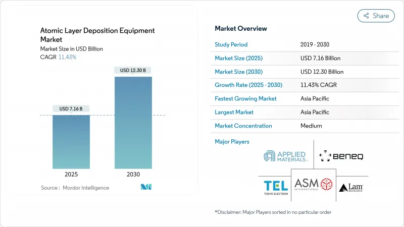
預計到 2025 年,原子層沉積 (ALD) 設備市場規模將達到 71.6 億美元,到 2030 年將達到 123 億美元,年複合成長率為 11.43%。
這項擴張主要受先進邏輯和3D儲存節點製程強度不斷提高、環柵(GAA)電晶體的普及以及固態電池和微型LED生產線需求激增的推動。亞太地區大規模晶圓廠的建設,加上美國和歐盟的政策獎勵,正在擴大單晶圓、批量和太空平台的需求。設備製造商透過引入高通量反應器、提供低電阻率金屬薄膜(例如釕和鉬)以及整合即時前驅體使用分析來獲取價值。同時,前驅體短缺、PFAS法規以及降低單晶圓成本的需求,正促使工具供應商和晶片製造商更加關注製程整合和供應鏈韌性。
全球原子層沉積(ALD)設備市場趨勢及洞察
亞洲3D NAND和DRAM製程節點快速縮小
商用3D NAND元件已超過200層,需要沉積數十層高長寬比的介電層和金屬層,沉積精度需達到亞埃級。韓國和中國的主要記憶體製造商對能夠將100:1長寬比結構的厚度偏差控制在1%以下的熱原子層沉積(ALD)反應器的訂單激增。記憶體價格在2024年至2025年間回升,帶動工廠運轉率恢復,儘管面臨出口限制的不利因素,設備需求依然強勁。 2024年,中國晶圓廠購入了全球40%的晶圓製造設備,導致ALD前驅體產能出現區域性供不應求。能夠兼顧批量經濟性和高介電常數均勻性的供應商獲得了最多的設備替換訂單。
全方位閘極設計及向高k金屬閘極邏輯的過渡
GAA架構將柵極電極移至奈米帶上,從而增加了每個裝置的共形高介電常數/金屬層數量。台積電的2nm平台計畫於2025年下半年量產,該平台簡化了數百道ALD製程步驟,與3nm節點相比,功耗降低了25-30%,同時確保了閾值電壓調節器。鉬和釕ALD已在某些互連層取代了鎢和銅,使線路電阻降低了35%,並簡化了CMP製程。市場需求偏向具有源內計量功能的單晶圓設備,該設備可在每個循環後檢驗薄膜厚度。能夠以每小時200瓦或更高的吞吐量提供2埃或更小的薄膜厚度重複性的供應商處於行業領先地位。
前驅金屬稀少與成本波動
釕和銥的供應鏈仍集中在兩個生產國,這意味著晶圓廠到2024年將面臨超過40%的價格波動。一家領先的邏輯晶圓廠由於釕短缺,將其3nm產推出推遲了三個月,並增加了一套前驅體回收裝置,導致設備資本支出增加了15%。鋅烷基輔助鈷原子層沉積(ALD)的研究已將薄片電阻降低至15µΩcm,但其電遷移壽命仍低於釕。在替代化學製程成熟之前,鉑族金屬(PGM)的價格將限制積極的成本削減藍圖。
細分市場分析
到2024年,熱感原子層沉積(ALD)將佔據ALD設備市場最大的佔有率,達到55.2%。單晶圓熱感反應器對於高深長寬比記憶體蝕刻停止層至關重要,其配方靈活性支援頻繁的前驅體更換。然而,太空ALD以17.1%的複合年成長率脫穎而出,成為2030年成長最快的技術。一家OLED面板製造商檢驗了大氣壓力空間ALD封裝,使其產能提高了四倍,並滿足了嚴格的阻隔性能指標。因此,每平方公尺成本下降了28%,新訂單也轉向了線上空間ALD設備。等離子體增強ALD擴大了其在軟性電子產品的應用範圍,使其能夠在低於100°C的溫度下進行沉積,這對於塑膠基板至關重要。供應商也推出了卷軸式版本,推動ALD技術應用於食品和太陽能組件的阻隔薄膜領域。
受顯示器和太陽能電池工廠需求的推動,用於太空原子層沉積(ALD)的設備市場規模預計將比其他任何領域更快成長。另一方面,支援原子層蝕刻(ALE)的平台已成為一個新的細分市場。透過將沉積和蝕刻整合到單一框架中,可以縮短232層NAND快閃記憶體的階梯蝕刻製程的等待時間。這些發展使收入來源不再局限於核心半導體領域。
叢集系統將佔2024年營收的65.2%,這得益於3奈米以下邏輯生產線配方的彈性。近期升級結合了先進的前驅體蒸汽輸送和機器學習故障檢測技術,使週期時間縮短了25%,晶圓間均勻性提高了40%。這些生產力的提升有助於單晶圓設備保持了其市場佔有率優勢。
然而,隨著記憶體和類比電路製造廠尋求降低單片晶圓成本,批式反應器正在重新興起。新型熱壁反應器設計可同時處理 100 片晶圓,並將溫度控制在 ±1°C 以內。一家韓國記憶體製造商將其介質襯墊製程從集群式原子層沉積 (ALD) 過渡到批量式 ALD 後,成本降低了 30%。因此,批量製程的收入以 14.3% 的複合年成長率成長,超過了整體市場的成長速度。
ALD(原子層沉積)設備市場報告按設備類型(熱 ALD、其他)、反應器配置(群集、獨立批次)、基板尺寸(小於 200 毫米、其他)、薄膜化學(氧化物、氮化物、氧氮化物、其他)、應用(半導體邏輯、記憶體、其他)和地區(北美、南美、歐洲、亞太、中東和非洲)進行細分。
區域分析
預計亞太地區在2024年將維持41.8%的營收佔有率,並在2030年前以17.3%的複合年成長率成長。台灣、韓國和中國大陸生產了全球80%以上的邏輯和儲存晶圓,從而集中了對晶圓製造設備的需求。儘管受到出口限制,但得益於470億美元的國家基金支持,僅中國大陸在2024年仍將採購全球40%的晶圓製造設備。該地區還擁有全球最高的微型LED產能,並日益廣泛地採用太空原子層沉積(ALD)技術。
北美則位居第二,這主要得益於CHIPS和科學法案的激勵措施。亞利桑那州、俄亥俄州和德克薩斯州的新建晶圓廠累計數十億美元用於GAA試點生產線和先進晶片封裝的ALD設備。美國企業將在2023年投入1,075億美元用於研發和資本支出,進而提振國內需求。
歐洲的佔有率雖小,但成長迅速。歐洲晶片計畫已籌集430億歐元(490.9億美元),其中包括37億歐元(42.2億美元)用於五條採用原子層沉積(ALD)技術進行先進封裝堆疊原型開發的試點生產線。巴西、以色列和阿拉伯聯合大公國的新活動拓展了客戶群,主要體現在針對電力電子和可再生能源儲存領域的研究。
其他福利:
- Excel格式的市場預測(ME)表
- 3個月的分析師支持
目錄
第1章 引言
- 研究假設和市場定義
- 調查範圍
第2章調查方法
第3章執行摘要
第4章 市場情勢
- 市場概覽
- 市場促進因素
- 亞洲3D NAND和DRAM製程節點快速縮小
- 向環柵(GAA)和高介電常數金屬閘極邏輯的過渡
- 快速採用迷你/微型LED背板
- 電動汽車電池用固體電解質被覆劑的需求
- 用於提高生物相容性的醫用植入奈米塗層
- 政府資助的試點生產線投資(歐盟晶片法案、晶片計畫、科學法案)
- 市場限制
- 前驅體金屬(Ru、Ir、Co)的稀少性與成本波動性
- 吞吐量限制和大批量晶圓代工廠目標
- OLED封裝空間CVD領域的競爭
- 氟化血漿製品的嚴格環境、健康與安全 (EHS) 法規
- 價值鏈分析
- 監理與技術展望
- 波特五力模型
- 供應商的議價能力
- 買方的議價能力
- 新進入者的威脅
- 替代品的威脅
- 競爭對手之間的競爭
- 宏觀經濟因素如何影響市場
第5章 市場規模與成長預測
- 透過裝置
- 熱感原子層沉積(批量)
- 等離子體增強原子層沉積(PEALD)
- 空間ALD
- 卷對卷/片對片原子層沉積
- 原子層蝕刻 (ALE) 相容工具
- 按反應器配置
- 叢集(單晶圓)
- 獨立批次
- 按基板尺寸
- 200毫米或更小
- 300 mm
- 450毫米或更長的導線
- 透過薄膜化學
- 氧化膜
- 氮化物和氧氮化物薄膜
- 金屬薄膜(Co、Ru、Ti、Al、Cu)
- 氟化物和硫化物薄膜
- 透過使用
- 半導體邏輯和記憶體
- 先進封裝和異構整合
- 功率和光電子(SiC、GaN、LED)
- 能源裝置(鋰離子電池、固體燃料電池)
- 生物醫學和植入表面功能化
- 汽車感測器和ADAS
- 按地區
- 北美洲
- 美國
- 加拿大
- 墨西哥
- 南美洲
- 巴西
- 阿根廷
- 其他南美洲
- 歐洲
- 德國
- 英國
- 法國
- 義大利
- 西班牙
- 俄羅斯
- 其他歐洲地區
- 亞太地區
- 中國
- 日本
- 印度
- 韓國
- 東南亞
- 亞太其他地區
- 中東和非洲
- 中東
- 沙烏地阿拉伯
- 阿拉伯聯合大公國
- 土耳其
- 其他中東地區
- 非洲
- 南非
- 奈及利亞
- 其他非洲地區
- 北美洲
第6章 競爭情勢
- 市場集中度
- 策略性舉措和合資分析
- 市佔率分析
- 公司簡介
- ASM International NV
- Applied Materials Inc.
- Tokyo Electron Limited
- Lam Research Corporation
- Veeco Instruments Inc.
- Oxford Instruments plc
- Beneq Oy
- Picosun Oy
- Entegris Inc.
- Kurt J. Lesker Company
- Hitachi High-Tech Corporation
- Ulvac Inc.
- Aixtron SE
- SENTECH Instruments GmbH
- CVD Equipment Corporation
- Forge Nano Inc.
- ALD NanoSolutions Inc.
- Lotus Applied Technology
- LPE SpA
- SVT Associates
- Arradiance LLC
- Beneq R2R(Service Business)
第7章 市場機會與未來展望
The atomic layer deposition equipment market size stood at USD 7.16 billion in 2025 and is forecast to reach USD 12.30 billion by 2030, reflecting an 11.43% CAGR.
This expansion has been propelled by rising process intensity at advanced logic and 3-D memory nodes, adoption of gate-all-around (GAA) transistors, and fast-growing demand from solid-state battery and micro-LED lines. Asia-Pacific's large wafer-fab build-out, coupled with policy incentives in the United States and European Union, has enlarged the buyer base for single-wafer, batch, and spatial platforms. Equipment makers are capturing value by introducing high-throughput reactors, offering lower-resistance metal films such as ruthenium and molybdenum, and embedding real-time precursor-utilization analytics. Meanwhile, precursor scarcity, PFAS regulation, and the need to trim cost-per-wafer keep process integration and supply-chain resilience at centre stage for tool vendors and chipmakers alike.
Global Atomic Layer Deposition Equipment Market Trends and Insights
Surging 3-D NAND and DRAM Node Shrink in Asia
Layer counts already surpassed 200 in commercial 3-D NAND devices, requiring dozens of high-aspect-ratio dielectric and metal layers deposited with sub-Angstrom precision. Leading memory makers in South Korea and China ramped orders for thermal ALD reactors that can maintain thickness variation below 1% across structures with 100:1 aspect ratios. Memory price recovery in 2024-2025 restored fab utilization, raising tool demand even amid export-control headwinds. Chinese fabs purchased 40% of global wafer-fab equipment in 2024, creating a regional undersupply of ALD precursor capacity. Vendors able to couple batch economics with high-k dielectric uniformity won most replacement awards.
Transition to Gate-All-Around and High-k Metal Gate Logic
GAA architectures move the gate electrode around the entire nanoribbon, multiplying the number of conformal high-k/metal layers per device. TSMC's 2 nm platform, slated for 2H 2025 mass production, integrates hundreds of ALD steps to secure threshold-voltage control while shaving 25-30% power versus 3 nm nodes. Molybdenum and ruthenium ALD replaced tungsten and copper in several interconnect levels, trimming line resistance by 35% and simplifying CMP. Demand has skewed toward single-wafer tools with in-source metrology that validates film thickness after every cycle. Suppliers capable of delivering sub-2 A thickness repeatability at >200 Wph throughput are best positioned.
Scarcity and Cost Volatility of Precursor Metals
Ruthenium and iridium supply chains remained concentrated in two producing nations, exposing fabs to price swings above 40% in 2024. One leading-edge logic fab deferred a 3 nm ramp by three months owing to Ru shortages, adding precursor-recycling skids that raised tool CAPEX by 15%. Research into zinc-alkyl-assisted cobalt ALD cut sheet resistance to 15 µΩ cm but still trails Ru in electromigration life. Until alternative chemistries mature, the price of PGMs will cap aggressive cost-down roadmaps.
Other drivers and restraints analyzed in the detailed report include:
- Rapid Adoption of Mini/Micro-LED Backplanes
- EV Battery Solid-State Electrolyte Coatings Demand
- Throughput Limitations vs. High-Volume Foundry Targets
For complete list of drivers and restraints, kindly check the Table Of Contents.
Segment Analysis
Thermal ALD captured the largest slice of the atomic layer deposition equipment market at 55.2% in 2024. Single-wafer thermal reactors proved indispensable for high-aspect-ratio memory etch-stop layers, with recipe flexibility supporting frequent precursor swaps. However, spatial ALD's 17.1% CAGR makes it the standout gainer through 2030. A top OLED panel maker validated atmospheric spatial ALD encapsulation that quadrupled throughput and met stringent barrier metrics. The resulting cost per square meter fell by 28%, steering fresh orders toward in-line spatial tools. Plasma-enhanced ALD widened its appeal for flexible electronics, enabling sub-100 °C film growth critical for plastic substrates. Vendors also released roll-to-roll variants, pushing ALD into barrier films for food and solar modules.
The atomic layer deposition equipment market size for Spatial ALD is projected to expand faster than any other segment, driven by demand from display and solar fabs. Conversely, ALE-enabled platforms surfaced as an emerging niche; integrating deposition and etch within one frame shortens process queues for 232-layer NAND stair-etch steps. Collectively, these developments diversified revenue streams beyond the core semiconductor base.
Cluster systems held 65.2% of 2024 revenue, favored for recipe agility at sub-3 nm logic lines. A recent upgrade that combined advanced precursor-vapor delivery with machine-learning fault detection trimmed cycle time 25% and boosted wafer-to-wafer uniformity 40%. Such productivity gains helped sustain the atomic layer deposition equipment market share advantage of single-wafer tools.
Batch reactors, however, are staging a comeback as memory and analog fabs seek lower cost per wafer. New hot-wall designs process 100 wafers simultaneously while controlling temperature within +-1 °C. A South Korean memory producer realized 30% cost savings when migrating a dielectric liner step from cluster to batch ALD. Consequently, batch revenue is on pace for a 14.3% CAGR, outstripping overall market growth.
The Atomic Layer Deposition Equipment Market Report is Segmented by Equipment Type (Thermal ALD, and More), by Reactor Configuration (Cluster, Stand-Alone Batch), by Substrate Size (<= 200 Mm, and More), by Film Chemistry (Oxide Films, Nitride and Oxy-Nitride Films, and More), by Application (Semiconductor Logic and Memory, and More), by Geography (North America, South America, Europe, Asia-Pacific, and Middle East and Africa).
Geography Analysis
Asia-Pacific retained a 41.8% revenue share in 2024 and is forecast to post a 17.3% CAGR through 2030. Taiwan, South Korea, and China jointly produced more than 80% of global logic and memory wafers, ensuring concentrated tool demand. China alone bought 40% of all wafer-fab equipment in 2024 despite export curbs, underpinned by a USD 47 billion national fund. The region also hosts most micro-LED capacity, further amplifying spatial ALD adoption.
North America ranked second, buoyed by CHIPS and the Science Act incentives. New fabs in Arizona, Ohio, and Texas earmarked multi-billion-dollar ALD tool budgets for GAA pilot lines and advanced chiplet packaging. U.S. firms invested USD 107.5 billion in research and development and capex during 2023, reinforcing domestic demand.
Europe's share is smaller yet accelerating. The European Chips Act mobilized EUR 43 billion (USD 49.09 billion), including EUR 3.7 billion (USD 4.22 billion) for five pilot lines that rely on ALD to prototype advanced packaging stacks. Emerging activity in Brazil, Israel, and the United Arab Emirates broadened the customer map, mainly through research lines targeting power electronics and renewable-energy storage.
- ASM International N.V.
- Applied Materials Inc.
- Tokyo Electron Limited
- Lam Research Corporation
- Veeco Instruments Inc.
- Oxford Instruments plc
- Beneq Oy
- Picosun Oy
- Entegris Inc.
- Kurt J. Lesker Company
- Hitachi High-Tech Corporation
- Ulvac Inc.
- Aixtron SE
- SENTECH Instruments GmbH
- CVD Equipment Corporation
- Forge Nano Inc.
- ALD NanoSolutions Inc.
- Lotus Applied Technology
- LPE S.p.A.
- SVT Associates
- Arradiance LLC
- Beneq R2R (Service Business)
Additional Benefits:
- The market estimate (ME) sheet in Excel format
- 3 months of analyst support
TABLE OF CONTENTS
1 INTRODUCTION
- 1.1 Study Assumptions and Market Definition
- 1.2 Scope of the Study
2 RESEARCH METHODOLOGY
3 EXECUTIVE SUMMARY
4 MARKET LANDSCAPE
- 4.1 Market Overview
- 4.2 Market Drivers
- 4.2.1 Surging 3-D NAND and DRAM Node Shrink in Asia
- 4.2.2 Transition to Gate-All-Around (GAA) and High-K Metal Gate Logic
- 4.2.3 Rapid Adoption of Mini/Micro-LED Backplanes
- 4.2.4 EV Battery Solid-State Electrolyte Coatings Demand
- 4.2.5 Medical Implant Nano-Coatings for Improved Bio-compatibility
- 4.2.6 Government-funded Pilot-Line Investments (EU Chips Act, CHIPS and Science Act)
- 4.3 Market Restraints
- 4.3.1 Scarcity and Cost Volatility of Precursor Metals (Ru, Ir, Co)
- 4.3.2 Throughput Limitations vs. High-Volume Foundry Targets
- 4.3.3 Competing Spatial CVD for OLED Encapsulation
- 4.3.4 Stringent EHS Regulations on Fluorinated Plasma By-products
- 4.4 Value Chain Analysis
- 4.5 Regulatory and Technological Outlook
- 4.6 Porter's Five Forces
- 4.6.1 Bargaining Power of Suppliers
- 4.6.2 Bargaining Power of Buyers
- 4.6.3 Threat of New Entrants
- 4.6.4 Threat of Substitutes
- 4.6.5 Intensity of Competitive Rivalry
- 4.7 Impact of Macroeconomic Factors on the market
5 MARKET SIZE AND GROWTH FORECASTS (VALUE)
- 5.1 By Equipment Type
- 5.1.1 Thermal ALD (Batch)
- 5.1.2 Plasma-Enhanced ALD (PEALD)
- 5.1.3 Spatial ALD
- 5.1.4 Roll-to-Roll / Sheet-to-Sheet ALD
- 5.1.5 Atomic Layer Etching (ALE)-Enabled Tools
- 5.2 By Reactor Configuration
- 5.2.1 Cluster (Single-Wafer)
- 5.2.2 Stand-alone Batch
- 5.3 By Substrate Size
- 5.3.1 <= 200 mm
- 5.3.2 300 mm
- 5.3.3 >= 450 mm Pilot Lines
- 5.4 By Film Chemistry
- 5.4.1 Oxide Films
- 5.4.2 Nitride and Oxy-Nitride Films
- 5.4.3 Metal Films (Co, Ru, Ti, Al, Cu)
- 5.4.4 Fluoride and Sulfide Films
- 5.5 By Application
- 5.5.1 Semiconductor Logic and Memory
- 5.5.2 Advanced Packaging and Heterogeneous Integration
- 5.5.3 Power and Optoelectronics (SiC, GaN, LEDs)
- 5.5.4 Energy Devices (Li-ion, Solid-State, Fuel Cells)
- 5.5.5 Biomedical and Implant Surface Functionalization
- 5.5.6 Automotive Sensors and ADAS
- 5.6 By Geography
- 5.6.1 North America
- 5.6.1.1 United States
- 5.6.1.2 Canada
- 5.6.1.3 Mexico
- 5.6.2 South America
- 5.6.2.1 Brazil
- 5.6.2.2 Argentina
- 5.6.2.3 Rest of South America
- 5.6.3 Europe
- 5.6.3.1 Germany
- 5.6.3.2 United Kingdom
- 5.6.3.3 France
- 5.6.3.4 Italy
- 5.6.3.5 Spain
- 5.6.3.6 Russia
- 5.6.3.7 Rest of Europe
- 5.6.4 Asia-Pacific
- 5.6.4.1 China
- 5.6.4.2 Japan
- 5.6.4.3 India
- 5.6.4.4 South Korea
- 5.6.4.5 South-East Asia
- 5.6.4.6 Rest of Asia-Pacific
- 5.6.5 Middle East and Africa
- 5.6.5.1 Middle East
- 5.6.5.1.1 Saudi Arabia
- 5.6.5.1.2 United Arab Emirates
- 5.6.5.1.3 Turkey
- 5.6.5.1.4 Rest of Middle East
- 5.6.5.2 Africa
- 5.6.5.2.1 South Africa
- 5.6.5.2.2 Nigeria
- 5.6.5.2.3 Rest of Africa
- 5.6.1 North America
6 COMPETITIVE LANDSCAPE
- 6.1 Market Concentration
- 6.2 Strategic Initiatives and JV Analysis
- 6.3 Market Share Analysis
- 6.4 Company Profiles (includes Global-level Overview, Market-level Overview, Core Segments, Financials as available, Strategic Information, Market Rank/Share, Products and Services, Recent Developments)
- 6.4.1 ASM International N.V.
- 6.4.2 Applied Materials Inc.
- 6.4.3 Tokyo Electron Limited
- 6.4.4 Lam Research Corporation
- 6.4.5 Veeco Instruments Inc.
- 6.4.6 Oxford Instruments plc
- 6.4.7 Beneq Oy
- 6.4.8 Picosun Oy
- 6.4.9 Entegris Inc.
- 6.4.10 Kurt J. Lesker Company
- 6.4.11 Hitachi High-Tech Corporation
- 6.4.12 Ulvac Inc.
- 6.4.13 Aixtron SE
- 6.4.14 SENTECH Instruments GmbH
- 6.4.15 CVD Equipment Corporation
- 6.4.16 Forge Nano Inc.
- 6.4.17 ALD NanoSolutions Inc.
- 6.4.18 Lotus Applied Technology
- 6.4.19 LPE S.p.A.
- 6.4.20 SVT Associates
- 6.4.21 Arradiance LLC
- 6.4.22 Beneq R2R (Service Business)
7 MARKET OPPORTUNITIES AND FUTURE OUTLOOK
- 7.1 White-space and Unmet-Need Assessment
 原子層沉澱設備市場(按設備類型、技術類型、應用和最終用戶產業分類)-2025-2032年全球預測原子層沉積市場(按設備類型、材料、應用和最終用戶產業)—全球預測 2025-2032
 2025年原子層沉澱全球市場報告2025年全球ALD設備市場報告
 原子層沉積 (ALD) 市場 - 全球產業規模、佔有率、趨勢、機會和預測(按類型、按材料、按最終用途行業、按地區和競爭細分,2020-2030 年)
 全球半導體 ALD 和 CVD 前驅市場
 原子層沉積 (ALD) 市場預測(至 2032 年):按產品類型、應用、最終用戶和地區進行的全球分析
 全球 ALD 設備市場研究報告 - 產業分析、規模、佔有率、成長、趨勢及 2025 年至 2033 年預測
 原子層沉積設備市場報告(按產品(金屬 ALD、氧化鋁 ALD、等離子體增強 ALD、催化 ALD 等)、應用(半導體、太陽能設備、電子產品、醫療設備等)和地區)2025 年至 2033 年全球原子層沉積市場研究報告-產業分析、規模、佔有率、成長、趨勢與預測 2025 年至 2033 年