


 |
市場調查報告書
商品編碼
1850222
自動測試機:市場佔有率分析、產業趨勢、統計數據和成長預測(2025-2030 年)Automated Test Equipment - Market Share Analysis, Industry Trends & Statistics, Growth Forecasts (2025 - 2030) |
||||||
※ 本網頁內容可能與最新版本有所差異。詳細情況請與我們聯繫。
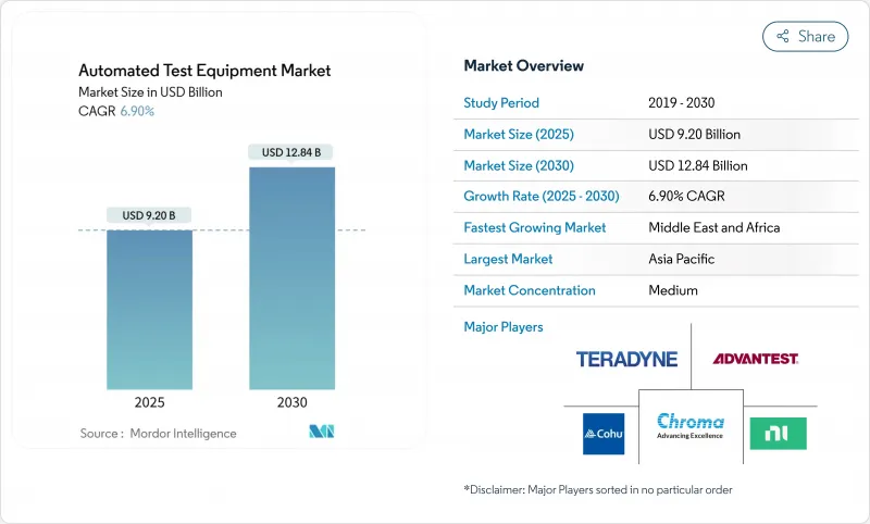
預計到 2025 年,自動化測試機市場規模將達到 92 億美元,到 2030 年將達到 128.4 億美元,年複合成長率為 6.9%。
需求成長的驅動力來自於向5奈米以下製程節點的過渡、汽車電氣化以及系統級封裝設計日益複雜的趨勢。製造商正在投資研發能夠測量10 nV/√Hz或更低雜訊的超低雜訊平台,而功率元件專家則指定使用能夠安全施加超過1200V應力的測試儀。設備供應商同時也在整合即時數據分析功能,以縮短調試週期並提高產量比率。在主要企業持續整合的同時,一些創新中型企業正瞄準諸如人工智慧加速器晶圓級老化測試和光電裝置可靠度檢驗等細分成長領域。
全球自動化測試設備市場趨勢與洞察
縮小到 7 奈米以下的製程節點需要超低雜訊的自動測試設備
台灣和韓國的7奈米以下製程製程正在蓬勃發展,對測量精度(低於10 nV/√Hz)和時序精度(皮秒級)提出了極高的要求。領先的代工廠正在透過驗證新型向量並行架構來應對這些挑戰,這些架構透過增強屏蔽和最佳化接地參考來抑制串擾。工具供應商正在將這些設計與機器學習主導的模式產生結合,以縮短特性分析週期,這項功能現在已成為主流SoC定序的標準配置。
汽車功能安全積體電路測試突波(ISO 26262)
一家歐洲一級半導體供應商在2024年至2025年間,故障注入測試儀的使用率提高了34%。該設備可執行數百種安全目標組合,並將結果對應到需求可追溯性矩陣。透過與硬體在環測試台整合,可以對動力傳動系統逆變器、雷達感測器和MCU子系統進行協同檢驗,從而大規模確保符合ASIL-D標準。
5nm以下測試儀資本密集度高,投資回收期長
與7nm製程相比,平台價格上漲了35%,中型晶圓廠的投資回收期超過五年。對超穩定低介電常數材料探測、先進熱調控以及多太Terabit圖形化記憶體的需求,推高了購置成本和服務成本,抑制了小型晶圓廠的採用率。
細分市場分析
到2024年,涵蓋邏輯、SoC和射頻元件的非記憶體測試儀將佔據自動化測試設備市場47.3%的佔有率。其市場主導地位源自於對人工智慧處理器、5G收發器和汽車網域控制器等產品的篩檢需求。供應商已將向量速度提升至每引腳5Gbps以上,並增加了亞太兆赫射頻選項以應對混合工作負載。基於機器學習的模式生成技術縮短了測試週期,使其適用於大批量智慧型手機和資料中心製造。整合的分析功能將故障特徵與佈局模組關聯起來,減少了返工,並鞏固了該細分市場的收入領先地位。
測試處理設備是成長最快的品類,預計從2025年到2030年將以11.4%的複合年成長率成長,這主要得益於汽車和電力線產業對更高吞吐量和更嚴格熱控制的需求。隨著晶圓廠指定使用多區域測試板和主動減振技術來驗證175°C下寬能能隙裝置的性能,測試處理設備的自動化測試市場規模正在擴大。先進的機器人技術現在可以移動易碎的3D堆疊封裝而不會產生微裂紋,從而提高了SiP組件的一次合格產量比率。預測性維護軟體進一步減少了停機時間,使該細分市場保持了兩位數的成長。
測試主機透過整合模式產生加速器和雲端連接分析模組的升級而得到加強,在 2024 年佔收入的 56.4%。介面板現在採用低損耗層壓板,支援 70Gbps 差分通道,主動式熱控制插座可將結溫穩定在 ±0.5°C 以內。
系統級/老化機架式自動化測試儀市場規模預計將以 12.9% 的複合年成長率成長,主要驅動力來自人工智慧加速器的晶圓級應力測試和光電組件檢驗。探針技術的創新使得 MEMS 彈簧探針卡能夠應對更小的墊片間距,並提供 3μm 的定位精度。夾具設計增加了多區域冷卻板,以滿足安全關鍵型汽車積體電路所需的擴展溫度測試矩陣。
自動化測試設備市場按測試設備類型(記憶體、非記憶體、離散、測試處理機)、組件(測試儀、處理機、探針台、其他)、測試階段(晶圓探針測試、其他)、技術節點(28 奈米以上、14-22 奈米、7-10 奈米、5 南美洲
區域分析
亞太地區,得益於台灣、韓國、中國當地和日本300mm晶圓廠的集中,引領了自動化測試設備市場,在2024年佔全球收入的62.4%。 3nm和2nm節點晶圓代工廠的擴張,帶動了新竹和京畿道等地對超低噪聲最終測試線的相應投資,而中國IDM企業則加快了國內探針台和處理台的採購,以抵消出口限制的影響。
在北美,CHIPS 法案的激勵措施使亞利桑那州、德克薩斯和紐約州的幾家待開發區工廠得以推進,從而對能夠處理零下 40°C 環境應力曲線的封裝/最終和系統級工作站產生了新的需求。
隨著德國和法國擴大ADAS處理器和電源模組的測試能力以及功能安全積體電路的生產,歐洲的市佔率有所成長。此外,總額達430億歐元的《歐洲晶片法案》旨在2030年將區域產量加倍,這將刺激對測試儀的相應訂單。
預計2025年至2030年,中東和非洲地區的複合年成長率將達到9.1%,主要得益於阿拉伯聯合大公國和沙烏地阿拉伯將多元化資金投入當地的射頻前端企業。南非和奈及利亞的非洲中心已為該地區的無新興企業推出了混合訊號測試台認證。
其他福利:
- Excel格式的市場預測(ME)表
- 3個月的分析師支持
目錄
第1章 引言
- 研究假設和市場定義
- 調查範圍
第2章調查方法
第3章執行摘要
第4章 市場情勢
- 市場概覽
- 市場促進因素
- 需要超低雜訊ATE的7nm以下節點
- 歐盟汽車功能安全積體電路測試(ISO 26262)快速成長
- SiC/GaN功率元件引領高壓分離式ATE的發展
- 系統級封裝(SiP) 的成長推動了系統級測試人員的發展
- 亞洲5G/6G射頻前端複雜性
- 回流獎勵(美國晶片製造激勵計畫、歐盟晶片製造激勵計畫法案)擴大偵測能力
- 市場限制
- 5nm以下製程的測試設備資本投入龐大,投資回收期長。
- 片上BIST降低了外部數字ATE的需求
- 供應商介面互通性有限
- 週期性半導體資本支出削減
- 價值鏈分析
- 監管/技術展望
- 波特五力模型
- 新進入者的威脅
- 買方的議價能力
- 供應商的議價能力
- 替代品的威脅
- 競爭對手之間的競爭
- 投資分析
- 宏觀經濟因素的影響
第5章 市場規模與成長預測
- 按測試設備類型
- 記憶
- DRAM
- 閃光
- 非記憶體
- 邏輯/SoC
- 混合訊號和模擬
- RF
- 離散的
- 測試處理程序
- 記憶
- 按組件
- 測試員(核心系統)
- 處理程式
- 探針
- 負載/介面板和插座
- 測試階段
- 晶圓探針測試
- 包裝/最終測試
- 系統級/老化測試
- 依技術節點
- 28奈米或更大
- 14-22 nm
- 7-10 nm
- 5奈米或更小
- 按最終用戶行業分類
- 消費性電子產品
- 資訊科技/通訊
- 汽車和電動車
- 航太與國防
- 醫療設備
- 工業與電力
- 按地區
- 北美洲
- 美國
- 加拿大
- 墨西哥
- 南美洲
- 巴西
- 阿根廷
- 其他南美洲
- 歐洲
- 德國
- 英國
- 法國
- 義大利
- 北歐國家(瑞典、芬蘭、挪威、丹麥)
- 其他歐洲地區
- 亞太地區
- 中國
- 日本
- 韓國
- 台灣
- 亞太其他地區
- 中東和非洲
- 中東
- 沙烏地阿拉伯
- 阿拉伯聯合大公國
- 土耳其
- 其他中東地區
- 非洲
- 南非
- 奈及利亞
- 其他非洲地區
- 北美洲
第6章 競爭情勢
- 市場集中度
- 策略趨勢
- 市佔率分析
- 公司簡介
- Advantest Corp.
- Cohu Inc.
- National Instruments(NI)
- FormFactor Inc.
- Hon Precision(Huafeng)
- TESEC Corp.
- Tokyo Electron(TEL)
- UniTest Inc.
- Shenzhen ChangHong Tech.
- Blue Chip Testers
- MAC Panel Company
- Star Technologies
- Samsung Semiconductor(Internal ATE)
- Teradyne Inc.
- Chroma ATE Inc.
- SPEA SpA
- Astronics Corp.
- InTest Corp.
- Toray Engineering
- Hangzhou ChangChuan Tech.
- Exicon Co.
- Leader Tech.
- Roos Instruments
- Virginia Panel Corp.
- Aeroflex Inc.(Cobham)
- Asset InterTech
第7章 市場機會與未來展望
The Automated Test Equipment market size was valued at USD 9.20 billion in 2025 and is projected to climb to USD 12.84 billion by 2030, advancing at a 6.9% CAGR.
Demand is propelled by the migration to sub-5 nm nodes, the electrification of vehicles, and the rising complexity of System-in-Package designs. Manufacturers are channelling capital toward ultra-low-noise platforms able to measure below 10 nV/√Hz, while power-device specialists are specifying testers that safely apply in excess of 1,200 V stresses. Equipment vendors are simultaneously integrating real-time data analytics to shorten debug cycles and improve yield learning. Consolidation among leading suppliers continues, yet innovative mid-tier companies are targeting niche growth pockets such as wafer-level burn-in for AI accelerators and photonics device reliability validation.
Global Automated Test Equipment Market Trends and Insights
Shrinking <7 nm Nodes Requiring Ultra-Low-Noise ATE
Sub-7 nm production ramp-ups in Taiwan and South Korea have mandated measurement precision below 10 nV/√Hz and picosecond-level timing. Leading foundries have responded by qualifying new vector-parallel architectures that suppress crosstalk through enhanced shielding and optimized ground referencing. Tool suppliers are pairing these designs with machine-learning-driven pattern generation to compress characterization loops, a feature now standard on flagship SoC platforms.
Automotive Functional-Safety IC Testing Surge (ISO 26262)
European Tier-1 semiconductor vendors increased deployments of fault-injection-capable testers by 34% between 2024 and 2025. The equipment executes hundreds of safety-goal permutations, mapping results back to requirements-traceability matrices. Integration with hardware-in-the-loop benches enables simultaneous verification of powertrain inverters, radar sensors, and MCU subsystems, ensuring ASIL-D compliance at scale.
High Capital Intensity and Lengthy Pay-Back for Sub-5 nm Testers
Platform prices rose 35% versus the 7 nm generation, stretching ROI beyond five years for mid-tier fabs. The need for ultra-stable low-k dielectric probing, advanced thermal regulation, and multi-terabit pattern memory inflates both acquisition and service costs, tempering adoption rates among smaller foundries.
Other drivers and restraints analyzed in the detailed report include:
- SiC / GaN Power Devices Driving High-Voltage Discrete ATE
- Growth of System-in-Package Fuelling System-Level Testers
- On-Chip BIST Reducing External Digital ATE Demand
For complete list of drivers and restraints, kindly check the Table Of Contents.
Segment Analysis
Non-memory testers covering logic, SoC, and RF devices captured 47.3% of the Automated Test Equipment market share in 2024. Their dominance arose from demand to screen AI processors, 5G transceivers, and automotive domain controllers. Vendors lifted vector speeds beyond 5 Gbps per pin and added sub-terahertz RF options to serve mixed workloads. Machine-learning pattern generation trimmed cycle times, suiting smartphone and data-centre volume runs. Integrated analytics linked fail signatures to layout blocks, reducing respins and cementing the segment's revenue lead.
Test handlers form the fastest-growing category, with an 11.4% CAGR projected from 2025 to 2030 as automotive and power lines seek higher throughput and tighter thermal control. The Automated Test Equipment market size for handlers is widening as fabs specify multi-zone plates and active vibration damping to qualify wide-bandgap devices at 175 °C. Advanced robotics now moves fragile 3D-stacked packages without micro-cracking, raising first-pass yield in SiP assembly. Predictive-maintenance software further trims downtime, sustaining the segment's double-digit trajectory.
Tester mainframes held 56.4% revenue in 2024, bolstered by upgrades that integrate pattern-generation accelerators and cloud-connected analytics modules. Interface boards now employ low-loss laminates to support 70 Gbps differential lanes, while active thermal-control sockets stabilize junction temperatures within +-0.5 °C.
Automated Test Equipment market size for system-level/burn-in racks is projected to rise at 12.9% CAGR, driven by AI accelerator wafer-level stress testing and photonics assembly validation. Prober innovations address shrinking pad pitches through MEMS spring-probe cards offering 3 μm positional accuracy. Handler designs add multi-zone chill plates to match extended temperature test matrices demanded by safety-critical automotive ICs.
Automated Test Equipment Market is Segmented by Test Equipment Type (Memory, Non - Memory, Discrete, and Test Handlers), by Component (Tester, Handler, Prober, and More), by Test Stage (Wafer Probe Test, and More), by Technology Node (>=28 Nm, 14-22 Nm, 7-10 Nm, and <=5 Nm), End-User Industry (Consumer Electronics, and More), and Geography (North America, South America, Europe, Asia-Pacific, Middle East and Africa).
Geography Analysis
Asia Pacific led the automated test equipment market with 62.4% revenue in 2024, supported by dense clusters of 300 mm fabs in Taiwan, South Korea, mainland China, and Japan. Foundry expansions at 3 nm and 2 nm nodes triggered corresponding investments in ultra-low-noise final-test lines across Hsinchu and Gyeonggi provinces, while Chinese IDMs accelerated domestic prober and handler procurement to offset export restrictions.
North America ranked second as CHIPS Act incentives advanced multiple green-field fabs in Arizona, Texas, and New York, creating fresh demand for package/final and system-level stations capable of ambient-minus-40 °C stress profiles; Mexico's automotive electronics corridor likewise upgraded handler fleets to serve nearby vehicle plants.
Europe's share increased on the back of functional-safety IC production, with Germany and France expanding test capacity for ADAS processors and power modules, while the EUR 43 billion European Chips Act aimed to double regional fabrication output by 2030, spurring parallel tester orders.
The Middle East and Africa are projected to post a 9.1% CAGR from 2025 to 2030 as the UAE and Saudi Arabia channel diversification funds into local RF-front-end ventures; African hubs in South Africa and Nigeria have begun qualifying mixed-signal benches for regional fabless start-ups.
- Advantest Corp.
- Cohu Inc.
- National Instruments (NI)
- FormFactor Inc.
- Hon Precision (Huafeng)
- TESEC Corp.
- Tokyo Electron (TEL)
- UniTest Inc.
- Shenzhen ChangHong Tech.
- Blue Chip Testers
- MAC Panel Company
- Star Technologies
- Samsung Semiconductor ( Internal ATE)
- Teradyne Inc.
- Chroma ATE Inc.
- SPEA SpA
- Astronics Corp.
- InTest Corp.
- Toray Engineering
- Hangzhou ChangChuan Tech.
- Exicon Co.
- Leader Tech.
- Roos Instruments
- Virginia Panel Corp.
- Aeroflex Inc. (Cobham)
- Asset InterTech
Additional Benefits:
- The market estimate (ME) sheet in Excel format
- 3 months of analyst support
TABLE OF CONTENTS
1 INTRODUCTION
- 1.1 Study Assumptions and Market Definition
- 1.2 Scope of the Study
2 RESEARCH METHODOLOGY
3 EXECUTIVE SUMMARY
4 MARKET LANDSCAPE
- 4.1 Market Overview
- 4.2 Market Drivers
- 4.2.1 Shrinking <7 nm Nodes Requiring Ultra-Low Noise ATE
- 4.2.2 Automotive Functional-Safety IC Testing (ISO 26262) Surge in EU
- 4.2.3 SiC / GaN Power Devices Driving High-Voltage Discrete ATE
- 4.2.4 Growth of System-in-Package (SiP) Fuelling System-Level Testers
- 4.2.5 5G / 6G RF Front-End Complexity in Asia
- 4.2.6 Reshoring Incentives (US CHIPS, EU Chips Acts) Expanding Test Capacity
- 4.3 Market Restraints
- 4.3.1 High Capital Intensity and Lengthy Pay-back for Sub-5 nm Testers
- 4.3.2 On-Chip BIST Reducing External Digital ATE Demand
- 4.3.3 Limited Inter-Vendor Interface Interoperability
- 4.3.4 Cyclical Semiconductor CAPEX Cuts
- 4.4 Value Chain Analysis
- 4.5 Regulatory / Technological Outlook
- 4.6 Porter's Five Forces
- 4.6.1 Threat of New Entrants
- 4.6.2 Bargaining Power of Buyers
- 4.6.3 Bargaining Power of Suppliers
- 4.6.4 Threat of Substitutes
- 4.6.5 Competitive Rivalry
- 4.7 Investment Analysis
- 4.8 Impact of Macroeconomic factors
5 MARKET SIZE AND GROWTH FORECASTS (VALUE)
- 5.1 By Test Equipment Type
- 5.1.1 Memory
- 5.1.1.1 DRAM
- 5.1.1.2 Flash
- 5.1.2 Non-Memory
- 5.1.2.1 Logic / SoC
- 5.1.2.2 Mixed-Signal and Analog
- 5.1.2.3 RF
- 5.1.3 Discrete
- 5.1.4 Test Handlers
- 5.1.1 Memory
- 5.2 By Component
- 5.2.1 Tester (Core System)
- 5.2.2 Handler
- 5.2.3 Prober
- 5.2.4 Load/Interface Boards and Sockets
- 5.3 By Test Stage
- 5.3.1 Wafer Probe Test
- 5.3.2 Package / Final Test
- 5.3.3 System-Level / Burn-in Test
- 5.4 By Technology Node
- 5.4.1 >=28 nm
- 5.4.2 14-22 nm
- 5.4.3 7-10 nm
- 5.4.4 <=5 nm
- 5.5 By End-User Industry
- 5.5.1 Consumer Electronics
- 5.5.2 IT and Telecommunications
- 5.5.3 Automotive and EV
- 5.5.4 Aerospace and Defense
- 5.5.5 Healthcare Devices
- 5.5.6 Industrial and Power
- 5.6 By Geography
- 5.6.1 North America
- 5.6.1.1 United States
- 5.6.1.2 Canada
- 5.6.1.3 Mexico
- 5.6.2 South America
- 5.6.2.1 Brazil
- 5.6.2.2 Argentina
- 5.6.2.3 Rest of South America
- 5.6.3 Europe
- 5.6.3.1 Germany
- 5.6.3.2 United Kingdom
- 5.6.3.3 France
- 5.6.3.4 Italy
- 5.6.3.5 Nordics (Sweden, Finland, Norway, Denmark)
- 5.6.3.6 Rest of Europe
- 5.6.4 Asia-Pacific
- 5.6.4.1 China
- 5.6.4.2 Japan
- 5.6.4.3 South Korea
- 5.6.4.4 Taiwan
- 5.6.4.5 Rest of Asia-Pacific
- 5.6.5 Middle East and Africa
- 5.6.5.1 Middle East
- 5.6.5.1.1 Saudi Arabia
- 5.6.5.1.2 United Arab Emirates
- 5.6.5.1.3 Turkey
- 5.6.5.1.4 Rest of Middle East
- 5.6.5.2 Africa
- 5.6.5.2.1 South Africa
- 5.6.5.2.2 Nigeria
- 5.6.5.2.3 Rest of Africa
- 5.6.1 North America
6 COMPETITIVE LANDSCAPE
- 6.1 Market Concentration
- 6.2 Strategic Moves
- 6.3 Market Share Analysis
- 6.4 Company Profiles (includes Global level Overview, Market level overview, Core Segments, Financials as available, Strategic Information, Market Rank/Share for key companies, Products & Services, and Recent Developments)
- 6.4.1 Advantest Corp.
- 6.4.2 Cohu Inc.
- 6.4.3 National Instruments (NI)
- 6.4.4 FormFactor Inc.
- 6.4.5 Hon Precision (Huafeng)
- 6.4.6 TESEC Corp.
- 6.4.7 Tokyo Electron (TEL)
- 6.4.8 UniTest Inc.
- 6.4.9 Shenzhen ChangHong Tech.
- 6.4.10 Blue Chip Testers
- 6.4.11 MAC Panel Company
- 6.4.12 Star Technologies
- 6.4.13 Samsung Semiconductor ( Internal ATE)
- 6.4.14 Teradyne Inc.
- 6.4.15 Chroma ATE Inc.
- 6.4.16 SPEA SpA
- 6.4.17 Astronics Corp.
- 6.4.18 InTest Corp.
- 6.4.19 Toray Engineering
- 6.4.20 Hangzhou ChangChuan Tech.
- 6.4.21 Exicon Co.
- 6.4.22 Leader Tech.
- 6.4.23 Roos Instruments
- 6.4.24 Virginia Panel Corp.
- 6.4.25 Aeroflex Inc. (Cobham)
- 6.4.26 Asset InterTech
7 MARKET OPPORTUNITIES AND FUTURE OUTLOOK
- 7.1 White-space and Unmet-Need Assessment
 自動化測試設備市場:依產品類型、測試技術、銷售管道和最終用戶產業分類-2026-2032年全球預測
 滾筒式測功機市場規模、佔有率和成長分析:按產品類型、車輛類型、應用、最終用戶和地區分類-2026-2033年產業預測
 2026年全球應用測試自動化市場報告2026年全球自動化測試設備市場報告航太自動化測試設備市場:按設備類型、測試類型、平台、技術和最終用戶分類,全球預測,2026-2032年全球多站點SLT測試處理程序市場(按產品類型、最終用戶和分銷管道分類)預測(2026-2032年)脂質氧化分析儀市場:2026-2032年全球預測(按檢測方法、技術、應用、便攜性和最終用戶分類)
 全球自動化測試設備市場:市場規模、佔有率、成長率、產業分析、依類型、應用和地區劃分的分析及預測(2026-2034年)
 應用測試自動化市場 - 全球產業規模、佔有率、趨勢、機會及預測(按測試類型、組織、部署、最終用戶、地區和競爭格局分類,2021-2031 年)自動化測試設備市場-全球產業規模、佔有率、趨勢、機會、預測:按組件、應用、類型、地區和競爭對手分類,2021-2031年