


 |
市場調查報告書
商品編碼
1850190
下一代記憶體:市場佔有率分析、行業趨勢、統計數據和成長預測(2025-2030 年)Next Generation Memory - Market Share Analysis, Industry Trends & Statistics, Growth Forecasts (2025 - 2030) |
||||||
※ 本網頁內容可能與最新版本有所差異。詳細情況請與我們聯繫。
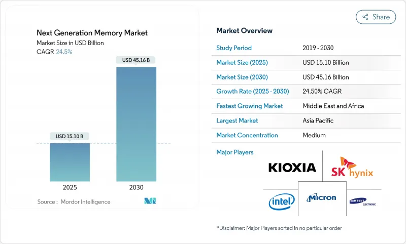
預計下一代記憶體市場將在 2025 年達到 151 億美元,在 2030 年達到 451.6 億美元,年複合成長率為 24.5%。
人工智慧訓練叢集、邊緣伺服器和自動駕駛汽車都面臨傳統DRAM-NAND架構的延遲限制,這加速了對記憶體的需求。為了彌合日益擴大的運算與記憶體之間的差距,廠商優先發展高頻寬架構、持久性儲存層級元件和先進封裝技術。亞太地區仍是製造強區,而北美晶圓廠則致力於提升並行產能。諸如Compute Express Link (CXL)和Universal Chiplet Interconnect Express (UCIe)等介面創新開始重新定義系統設計理念,推動記憶體池的分類,其擴展能力幾乎與加速器的數量呈線性關係。然而,高階製程節點和晶圓供應的限制仍然影響著下一代記憶體市場的定價和分配策略。
全球下一代記憶體市場趨勢與洞察
AI主導的超大規模資料中心對HBM的需求
變壓器架構的爆炸性成長迫使雲端營運商將其伺服器級 DRAM 和固態硬碟預算翻倍,頻寬而非容量成為主要瓶頸。高頻寬記憶體使鏈路吞吐量翻倍至 1.5 TB/s 以上,並顯著降低了每位元傳輸的能耗。 SK 海力士報告稱,其 2025 年的 HBM 供應已提前售罄,導致全球配額收緊,並促使 2026 年的長期訂單預訂。美光的觀察表明,AI 伺服器的 DRAM 容量將約為傳統 x86 節點的兩倍。這使得下一代記憶體市場從以位元成本為主導轉向以頻寬主導,從而為高階定價層級和更高的利潤率創造了機會。
汽車L4 ADAS需要即時啟動持久內存
L4級自動駕駛要求在斷電事件後能夠確定性地恢復,並能承受超過150°C的嚴苛動作溫度。鐵電存取記憶體(FRAM)裝置可在無待機電源的情況下承受10<sup>14</sup>次循環並保持資料完整性,從而確保感測器融合堆疊在冷啟動時仍能以高達100GB/s的速率運作。目前,汽車製造商正在評估將FRAM與LPDDR5X墊片結合的非對稱持久性非揮發性混合記憶體。這些架構能夠保護任務日誌,支援空中升級,並滿足ISO 26262的功能安全目標,推動下一代記憶體市場在整個移動出行價值鏈中的成長。
汽車PCM的熱穩定性問題
相變合金在150°C以上的高溫下難以維持數據,這會危及部署在沙漠或汽車引擎蓋下的事件記錄器的完整性。材料工程領域已探索了富鍺GeSbTe和串行PCM單元對,將耐久性窗口提升至153°C,但這增加了光刻步驟和成本。因此,OEM廠商的認證週期減緩了PCM的普及,在滿足可靠性目標之前,近期的設計訂單已轉向FRAM和ReRAM。這項限制正在抑制整體成長,尤其是在下一代記憶體市場的汽車細分領域。
細分市場分析
到2024年,揮發性記憶體將佔總收入的85.6%,這主要得益於HBM容量的顯著溢價。隨著AI加速器效能逐漸飽和至1TB/s以下,HBM的採購承諾將跨越多個會計年度,因此這項優勢依然存在。下一代易失性記憶體市場規模預計將繼續擴大,但隨著ReRAM、PCM和MRAM在邊緣運算和計量工作負載中日益普及,其市場佔有率將會下降。 ReRAM引領非揮發性記憶體的發展勢頭,憑藉其簡單的金屬-氧化物堆疊結構,無需額外掩模即可在28nm節點上進行共製造,其複合年成長率高達38.3%。 PCM的熱穩定性不斷提升,一旦通過10年150°C保持率的認證,預計將推動其在汽車產業的應用。 MRAM的進步與未來EUV微影技術的產能提升和製程簡化密切相關,這將縮小其相對於NAND快閃記憶體的每位元溢價。
在架構方面,易失性記憶體製造商目前正在探索堆疊式晶片拓撲結構,以減少晶粒面積並分散產量比率風險。非揮發性記憶體的挑戰則透過交叉點陣列和無選擇器設計來解決,這些設計無需使用佔用面積較大的電晶體。雖然隨著ReRAM和PCM供應加速,預計在預測期內揮發性記憶體的市佔率將下降約10個百分點,但隨著人工智慧伺服器總面積管理記憶體(TAM)翻番,易失性記憶體的絕對收入將會增加。設計人員將繼續整合晶粒和非揮發性晶粒,從而形成兼顧耐久性和永續性的混合堆疊結構。這些動態將確保多節點藍圖的實施,並擴大下一代記憶體市場解決方案的多樣性。
在單晶片矽技術出現之前,這種介面已經適應了對頻寬頻寬極高的加速器。 2024年,DDR和LPDDR通道的市佔率維持在38.3%,但每個插槽最多只能支援四個通道。透過PCIe 5.0實現CXL的連貫一致性連線緩解了這個限制,將Terabyte記憶體匯集到一個共用交換器後,並減少了單一記憶體的容量。 2024年8月發布的UCie 2.0規範提供了3D堆疊晶片,其頻寬晶粒前幾代產品的75倍,使得超大規模資料中心能夠在單一HBM堆疊上部署數十個運算晶粒。
展望未來,到2025年,50%的新型高效能運算(HPC)晶片流片將採用2.5D或3D晶片晶粒技術,CXL或UCIe將成為必備設計元素而非可選元素。重定時中心和重定時器將成為新的利潤來源。與這些轉變同步,PCIe/NVMe將繼續逐步實現世代更替,而SATA將逐漸退出市場,成為一種過時的介面。總體而言,新的介面將推動模組化設計的應用,使容量規劃與CPU升級週期脫鉤,並為下一代記憶體市場的多元化發展提供更多選擇。
下一代記憶體市場按技術(易失性、非揮發性)、記憶體介面(DDR/LPDDR、PCIe/NVMe、SATA、其他(CXL、Ucie))、終端設備(消費性電子產品、企業儲存和資料中心、汽車電子和ADAS、其他)、晶圓尺寸(200毫米以下、300毫米、450毫米和ADAS、其他)、晶圓尺寸(200毫米以下、300毫米、450毫米和美國地區細分(北美歐洲地區和美國地區)。
區域分析
亞太地區持續保持領先地位,預計2024年營收成長率將達到47.3%,三星、SK海力士和台積電等公司在下一代製程節點上的總合總額將超過850億美元。中國憑藉國家補貼和優惠融資政策,將國內DRAM產能提升至全球市場佔有率的5%,併計劃於2025年達到10%。日本延長了補貼政策,以維持其本土NAND快閃記憶體生產和專用設備叢集。印度推出了一項製造業激勵計劃,旨在吸引合資企業參與組裝、測試以及最終的3D NAND切片技術。這種區域深度佈局確保了供應安全,並促進了下一代記憶體市場的規模化利用。
北美晶片獎勵(CHIPS) 促進了美光公司位於愛達荷州的 HBM 晶圓廠和德克薩斯的記憶體組裝中心的發展,從而保障了國內國防和超大規模採購所需的產能。墨西哥則確保了後端組裝流程,與美國的前端晶圓生產形成互補。加拿大研究機構為超低功耗非揮發性材料的材料科學突破做出了貢獻,擴大了北美大陸的研發影響力。
歐洲在《半導體法》的指導下追求戰略自主,目標是到2030年佔據20%的全球市場佔有率。德國津貼了一個汽車級記憶體聯盟,法國投資了一條ReRAM試點生產線,英國優先發展與晶圓晶粒晶粒的晶片級晶片互連技術智慧財產權。歐盟尋求加強汽車製造商與本地記憶體廠商之間的合作,以增強下一代記憶體市場的區域需求。
中東和非洲的成長速度最快,預計年複合成長率將達到31.2%,這主要得益於沙烏地阿拉伯和阿拉伯聯合大公國主權財富基金支持的工廠。土耳其將自身定位為歐亞大陸的封裝中心,而南非則利用不斷成長的通訊密度來推動消費者對記憶體的需求。儘管基數不大,但積極的資本投入和勞動力技能提升表明,該地區下一代記憶體的市場佔有率將繼續成長。
其他福利:
- Excel格式的市場預測(ME)表
- 3個月的分析師支持
目錄
第1章 引言
- 研究假設和市場定義
- 調查範圍
第2章調查方法
第3章執行摘要
第4章 市場情勢
- 市場概覽
- 市場促進因素
- 人工智慧主導的超大規模資料中心對高頻寬記憶體的需求
- 汽車L4 ADAS中對即時開啟持久記憶體的需求
- 智慧型手機轉換到LPDDR5X和嵌入式ReRAM
- 國家記憶在地化計劃
- 工業邊緣物聯網需要超低功耗FRAM
- 基於 3D XPoint 的資料隱私主導持久記憶體內
- 市場限制
- 450mm 晶圓延遲限制了 ReRAM 的放大
- 與NAND快閃記憶體相比,MRAM的每位元成本更高。
- 汽車級相變材料熱穩定性差
- 28nm 以下 STT-MRAM晶圓代工廠集中度
- 價值鏈分析
- 監理與技術展望
- 波特五力模型
- 新進入者的威脅
- 買方的議價能力
- 供應商的議價能力
- 替代品的威脅
- 競爭對手之間的競爭
- 新興儲存技術藍圖分析
- 影響市場的宏觀經濟因素
第5章 市場規模與成長預測
- 透過技術
- 非揮發性
- 相變記憶體(PCM)
- 自旋轉移磁隨機存取記憶體(STT-MRAM)
- 切換 MRAM
- 阻變式隨機存取記憶體(ReRAM)
- 3D XPoint/Optan
- 鐵電存取記憶體(FeRAM)
- 奈米隨機存取記憶體
- 易揮發的
- 高頻寬記憶體(HBM)
- 混合儲存立方體(HMC)
- 低功耗 DDR5/LPDDR5X
- 非揮發性
- 透過記憶體介面
- DDR/LPDDR
- PCIe/NVMe
- SATA
- 其他(CXL、UCIe)
- 按最終用途設備
- 消費性電子產品
- 企業儲存與資料中心
- 汽車電子和ADAS
- 工業物聯網和製造業自動化
- 航太與國防
- 醫療保健和醫療設備
- 其他(智慧卡、穿戴式裝置)
- 按晶圓尺寸
- 200毫米或更小
- 300 mm
- 450 mm
- 按地區
- 北美洲
- 美國
- 加拿大
- 墨西哥
- 南美洲
- 巴西
- 阿根廷
- 其他南美洲
- 歐洲
- 德國
- 英國
- 法國
- 其他歐洲地區
- 亞太地區
- 中國
- 日本
- 韓國
- 印度
- 亞太其他地區
- 中東和非洲
- 中東
- 沙烏地阿拉伯
- 阿拉伯聯合大公國
- 土耳其
- 其他中東地區
- 非洲
- 南非
- 奈及利亞
- 其他非洲地區
- 北美洲
第6章 競爭情勢
- 市場集中度
- 策略趨勢
- 市佔率分析
- 公司簡介
- Samsung Electronics Co., Ltd.
- SK Hynix Inc.
- Micron Technology, Inc.
- Kioxia Holdings Corporation
- Intel Corporation
- Western Digital Corporation
- Everspin Technologies, Inc.
- Crossbar Inc.
- Avalanche Technology Inc.
- Spin Memory, Inc.
- Nantero Inc.
- Weebit Nano Ltd.
- Renesas Electronics Corporation
- Infineon Technologies AG
- NXP Semiconductors NV
- Changxin Memory Technologies(CXMT)
- Taiwan Semiconductor Manufacturing Co. Ltd.
- GlobalFoundries Inc.
- Winbond Electronics Corporation
- Macronix International Co., Ltd.
- Nanya Technology Corporation
- Advanced Semiconductor Engineering(ASE)Inc.
- Powerchip Semiconductor Manufacturing Corp.
- Yangtze Memory Technologies Co.(YMTC)
- Microchip Technology Inc.
第7章 市場機會與未來展望
The Next Generation Memory market size was valued at USD 15.10 billion in 2025 and is forecast to reach USD 45.16 billion by 2030, reflecting a vigorous 24.5% CAGR.
Demand accelerated as AI training clusters, edge servers, and autonomous vehicles all confronted the latency wall of conventional DRAM-NAND hierarchies. Vendors prioritized high-bandwidth architectures, persistent storage class devices, and advanced packaging to close the widening compute-to-memory gap. Asia-Pacific remained the production powerhouse, while North American fab incentives fostered parallel capacity. Interface innovations such as Compute Express Link (CXL) and Universal Chiplet Interconnect Express (UCIe) have begun to redraw system design philosophies, encouraging disaggregated memory pools that scale almost linearly with accelerator count. Supply constraints for premium nodes and wafers, however, continued to shape pricing and allocation strategies across the Next Generation Memory market.
Global Next Generation Memory Market Trends and Insights
AI-driven demand for HBM in hyperscale data centres
Surging transformer model sizes forced cloud operators to double server-level DRAM and solid-state budgets, making bandwidth rather than capacity the primary bottleneck. High Bandwidth Memory multiplied link throughput beyond 1.5 TB/s and delivered dramatic energy savings per bit moved. Global allocation tightened when SK Hynix reported its entire 2025 HBM output sold in advance, which prompted long-term volume reservations for 2026. Micron observed that an AI server deploys nearly twice the DRAM of a classic x86 node. The Next Generation Memory market, therefore, pivoted from bit-cost leadership toward bandwidth leadership, creating premium pricing tiers and margin expansion opportunities.
Automotive L4 ADAS needs instant-on persistent memory
Level 4 autonomy demands deterministic recovery after power events and harsh operating temperatures beyond 150 °C. Ferroelectric RAM devices withstand 1014 cycles while retaining data without standby power, ensuring cold-start availability for sensor fusion stacks that generate up to 100 GB/s. Automakers now evaluate asymmetric persistent-volatile hybrids combining FRAM with LPDDR5X scratch pads. These architectures protect mission logs, facilitate over-the-air updates, and support functional safety goals under ISO 26262, reinforcing growth in the Next Generation Memory market across the mobility value chain.
Thermal stability failures of automotive-grade PCM
Phase-change alloys struggled to retain data above 150 °C, jeopardizing event recorder integrity in desert and under-hood deployments. Material engineering explored Ge-rich GeSbTe and serial PCM cell pairs that push endurance windows to 153 °C but add lithography steps and cost. OEM qualification cycles, therefore, slowed PCM adoption, shifting near-term design wins to FRAM and ReRAM until reliability goals are met. The constraint compressed overall growth, particularly within the automotive subset of the Next Generation Memory market.
Other drivers and restraints analyzed in the detailed report include:
- Smartphone migration to LPDDR5X and embedded ReRAM
- National memory localization programs
- Foundry concentration for sub-28 nm STT-MRAM
For complete list of drivers and restraints, kindly check the Table Of Contents.
Segment Analysis
Volatile devices delivered 85.6% of 2024 revenue, anchored by HBM's steep capacity premiums. That dominance has persisted because AI accelerators saturate anything below 1 TB/s, ensuring HBM purchase commitments stretch multiple fiscal years. The Next Generation Memory market size for volatile solutions is projected to keep expanding in absolute terms even while share slips, as ReRAM, PCM, and MRAM gain credibility in edge and instrumentation workloads. ReRAM leads non-volatile momentum, growing at 38.3% CAGR thanks to simple metal-oxide stacks that co-fabricate on 28 nm nodes without extra masks. PCM's gradual thermal-stability gains are expected to unlock automotive attach once the 10-year, 150 °C retention benchmark is certified. MRAM advances remain tied to future EUV capacity and to process simplification that narrows the per-bit premium versus NAND.
Structurally, volatile makers now explore stacked chiplet topologies, trimming die area, and spreading yield risk. Non-volatile challengers respond with cross-point arrays and selector-less designs that eliminate area-consuming transistors. Over the outlook period, supply acceleration for ReRAM and PCM is expected to erode volatile share by roughly 10 percentage points, although absolute volatile revenue still rises because the AI server TAM doubles. Designers will continue to co-package volatile and non-volatile dies, cultivating hybrid stacks that trade endurance for persistence. Those dynamics ensure a multi-node roadmap, widening solution diversity within the Next Generation Memory market.
Interfaces adapted to bandwidth-hungry accelerators long before monolithic silicon could keep pace. In 2024, DDR and LPDDR channels retained a 38.3% share, but adoption ceilings emerged at four channels per socket. CXL's cache-coherent attach over PCIe 5.0 eased that limit, pooling terabytes of memory behind shared switches and slashing stranded capacity. The arrival of the UCIe 2.0 spec in August 2024 delivered 3D-stacked chiplets with 75 X the prior inter-die bandwidth, empowering hyperscalers to tile dozens of compute dies against a single HBM stack.
Looking ahead, 50% of new HPC tape-outs in 2025 will embed 2.5D or 3D die-to-die links, elevating CXL or UCIe from optional to mandatory design elements. Retiming hubs and retimers emerge as ancillary profit pools. Synchronous to these shifts, PCIe/NVMe continues incremental generational moves, but SATA fades toward archival niches. Collectively, novel interfaces propel modular deployments that decouple capacity planning from CPU upgrade cycles, enlarging diversification options within the Next Generation Memory market.
Next Generation Memory Market is Segmented by Technology (Volatile, and Non-Volatile), by Memory Interface (DDR/LPDDR, PCIe/NVMe, SATA, and Others (CXL, Ucie)), by End-Use Device (Consumer Electronics, Enterprise Storage and Data Centers, Automotive Electronics and ADAS, and More), by Wafer Size (<= 200 Mm, 300 Mm, and 450 Mm), and by Geography (North America, South America, Europe, Asia-Pacific, and Middle East and Africa).
Geography Analysis
Asia-Pacific maintained its leadership with 47.3% revenue in 2024, sustained by Samsung, SK Hynix, and TSMC, whose combined capital plans exceeded USD 85 billion for next-generation nodes. China advanced its indigenous DRAM capacity to a 5% global share and targeted 10% by 2025, guided by state grants and preferential loan terms. Japan's renewed subsidies preserved local NAND output and specialty equipment clusters. India launched fabrication incentive programs that attracted joint ventures geared toward assembly, test, and eventually 3D NAND slicing. This regional depth anchored supply security and fostered volume leverage for the Next Generation Memory market.
North America's CHIPS incentive catalysed Micron's Idaho HBM fab and Texas memory assembly centres, ensuring domestic capacity for defense and hyperscale procurement. Mexico captured backend assembly flows, complementing the United States front-end wafer starts. Canadian institutes contributed materials science breakthroughs aimed at ultra-low-power non-volatiles, expanding the research and development halo of the continent.
Europe pursued strategic autonomy under its semiconductor act, targeting a 20% global share by 2030. Germany funnelled grants toward automotive-grade memory consortia, while France invested in ReRAM pilot lines. The United Kingdom prioritized foundry-agnostic IP for chiplet die-to-die fabrics. Collectively, the bloc sought tighter integration between automotive OEMs and local memory houses, reinforcing regional demand in the Next Generation Memory market.
The Middle East and Africa exhibited the fastest trajectory, with a 31.2% CAGR outlook underpinned by sovereign wealth-fund backed fabs in Saudi Arabia and the UAE. Turkey marketed itself as a Eurasian packaging hub, and South Africa leveraged telecom densification to spur consumer memory uptake. While the base is modest, aggressive capital allocations and labour-force upskilling suggest durable upside for the region's share of the Next Generation Memory market.
- Samsung Electronics Co., Ltd.
- SK Hynix Inc.
- Micron Technology, Inc.
- Kioxia Holdings Corporation
- Intel Corporation
- Western Digital Corporation
- Everspin Technologies, Inc.
- Crossbar Inc.
- Avalanche Technology Inc.
- Spin Memory, Inc.
- Nantero Inc.
- Weebit Nano Ltd.
- Renesas Electronics Corporation
- Infineon Technologies AG
- NXP Semiconductors N.V.
- Changxin Memory Technologies (CXMT)
- Taiwan Semiconductor Manufacturing Co. Ltd.
- GlobalFoundries Inc.
- Winbond Electronics Corporation
- Macronix International Co., Ltd.
- Nanya Technology Corporation
- Advanced Semiconductor Engineering (ASE) Inc.
- Powerchip Semiconductor Manufacturing Corp.
- Yangtze Memory Technologies Co. (YMTC)
- Microchip Technology Inc.
Additional Benefits:
- The market estimate (ME) sheet in Excel format
- 3 months of analyst support
TABLE OF CONTENTS
1 INTRODUCTION
- 1.1 Study Assumptions and Market Definition
- 1.2 Scope of the Study
2 RESEARCH METHODOLOGY
3 EXECUTIVE SUMMARY
4 MARKET LANDSCAPE
- 4.1 Market Overview
- 4.2 Market Drivers
- 4.2.1 AI-Driven Demand for HBM in Hyperscale Data Centers
- 4.2.2 Automotive L4 ADAS Need for Instant-On Persistent Memory
- 4.2.3 Smartphone Migration to LPDDR5X and Embedded ReRAM
- 4.2.4 National Memory Localization Programs
- 4.2.5 Industrial Edge-IoT Requiring Ultra-Low-Power FRAM
- 4.2.6 Data-Privacy-Driven Persistent In-Memory Databases Using 3D XPoint
- 4.3 Market Restraints
- 4.3.1 450 mm Wafer Delay Constraining ReRAM Scale-up
- 4.3.2 High Per-Bit MRAM Cost versus NAND
- 4.3.3 Thermal Stability Failures of Automotive-Grade PCM
- 4.3.4 Foundry Concentration for Sub-28 nm STT-MRAM
- 4.4 Value Chain Analysis
- 4.5 Regulatory and Technological Outlook
- 4.6 Porter's Five Forces
- 4.6.1 Threat of New Entrants
- 4.6.2 Bargaining Power of Buyers
- 4.6.3 Bargaining Power of Suppliers
- 4.6.4 Threat of Substitutes
- 4.6.5 Competitive Rivalry
- 4.7 Emerging Memory Technology Roadmap Analysis
- 4.8 Impact of Macroeconomic factors on the Market
5 MARKET SIZE AND GROWTH FORECASTS (VALUE)
- 5.1 By Technology
- 5.1.1 Non-Volatile
- 5.1.1.1 Phase-Change Memory (PCM)
- 5.1.1.2 Spin-Transfer MRAM (STT-MRAM)
- 5.1.1.3 Toggle MRAM
- 5.1.1.4 Resistive RAM (ReRAM)
- 5.1.1.5 3D XPoint / Optane
- 5.1.1.6 Ferroelectric RAM (FeRAM)
- 5.1.1.7 NanoRAM
- 5.1.2 Volatile
- 5.1.2.1 High-Bandwidth Memory (HBM)
- 5.1.2.2 Hybrid Memory Cube (HMC)
- 5.1.2.3 Low-Power DDR5 / LPDDR5X
- 5.1.1 Non-Volatile
- 5.2 By Memory Interface
- 5.2.1 DDR / LPDDR
- 5.2.2 PCIe / NVMe
- 5.2.3 SATA
- 5.2.4 Others (CXL, UCIe)
- 5.3 By End-Use Device
- 5.3.1 Consumer Electronics
- 5.3.2 Enterprise Storage and Data Centers
- 5.3.3 Automotive Electronics and ADAS
- 5.3.4 Industrial IoT and Manufacturing Automation
- 5.3.5 Aerospace and Defense
- 5.3.6 Healthcare and Medical Devices
- 5.3.7 Others (Smart Cards, Wearables)
- 5.4 By Wafer Size
- 5.4.1 <= 200 mm
- 5.4.2 300 mm
- 5.4.3 450 mm
- 5.5 By Geography
- 5.5.1 North America
- 5.5.1.1 United States
- 5.5.1.2 Canada
- 5.5.1.3 Mexico
- 5.5.2 South America
- 5.5.2.1 Brazil
- 5.5.2.2 Argentina
- 5.5.2.3 Rest of South America
- 5.5.3 Europe
- 5.5.3.1 Germany
- 5.5.3.2 United Kingdom
- 5.5.3.3 France
- 5.5.3.4 Rest of Europe
- 5.5.4 Asia-Pacific
- 5.5.4.1 China
- 5.5.4.2 Japan
- 5.5.4.3 South Korea
- 5.5.4.4 India
- 5.5.4.5 Rest of Asia-Pacific
- 5.5.5 Middle East and Africa
- 5.5.5.1 Middle East
- 5.5.5.1.1 Saudi Arabia
- 5.5.5.1.2 United Arab Emirates
- 5.5.5.1.3 Turkey
- 5.5.5.1.4 Rest of Middle East
- 5.5.5.2 Africa
- 5.5.5.2.1 South Africa
- 5.5.5.2.2 Nigeria
- 5.5.5.2.3 Rest of Africa
- 5.5.1 North America
6 COMPETITIVE LANDSCAPE
- 6.1 Market Concentration
- 6.2 Strategic Moves
- 6.3 Market Share Analysis
- 6.4 Company Profiles {(includes Global level Overview, Market level overview, Core Segments, Financials as available, Strategic Information, Market Rank/Share for key companies, Products and Services, and Recent Developments)}
- 6.4.1 Samsung Electronics Co., Ltd.
- 6.4.2 SK Hynix Inc.
- 6.4.3 Micron Technology, Inc.
- 6.4.4 Kioxia Holdings Corporation
- 6.4.5 Intel Corporation
- 6.4.6 Western Digital Corporation
- 6.4.7 Everspin Technologies, Inc.
- 6.4.8 Crossbar Inc.
- 6.4.9 Avalanche Technology Inc.
- 6.4.10 Spin Memory, Inc.
- 6.4.11 Nantero Inc.
- 6.4.12 Weebit Nano Ltd.
- 6.4.13 Renesas Electronics Corporation
- 6.4.14 Infineon Technologies AG
- 6.4.15 NXP Semiconductors N.V.
- 6.4.16 Changxin Memory Technologies (CXMT)
- 6.4.17 Taiwan Semiconductor Manufacturing Co. Ltd.
- 6.4.18 GlobalFoundries Inc.
- 6.4.19 Winbond Electronics Corporation
- 6.4.20 Macronix International Co., Ltd.
- 6.4.21 Nanya Technology Corporation
- 6.4.22 Advanced Semiconductor Engineering (ASE) Inc.
- 6.4.23 Powerchip Semiconductor Manufacturing Corp.
- 6.4.24 Yangtze Memory Technologies Co. (YMTC)
- 6.4.25 Microchip Technology Inc.
7 MARKET OPPORTUNITIES AND FUTURE OUTLOOK
- 7.1 White-Space and Unmet-Need Assessment
 下一代記憶體市場:按技術、晶圓尺寸、應用和終端用戶產業分類-2026-2032年全球市場預測
 下一代記憶體市場規模、佔有率、趨勢和預測:按技術、晶圓尺寸、儲存類型、應用和地區分類(2026-2034 年)
 下一代記憶體市場規模、佔有率和成長分析(按技術、晶圓尺寸、應用和地區分類)—2026-2033年產業預測
 2026-2030年全球記憶體IC市場
 下一代儲存技術市場分析及預測(至2035年):按類型、產品類型、技術、應用、組件、形狀、材質、裝置、最終用戶和功能分類
 記憶體IC市場規模、佔有率及成長分析(按類型、終端用戶產業及地區分類)-2026-2033年產業預測
 下一代記憶體市場-2025-2030年預測記憶體IC市場-2025-2030年預測
 全球下一代記憶體技術市場(按技術、垂直行業和地區分類)
 記憶體 IC:市場佔有率分析、行業趨勢和統計、成長預測(2025-2030 年)