


 |
市場調查報告書
商品編碼
1849988
光電:市場佔有率分析、行業趨勢、統計數據和成長預測(2025-2030 年)Photonics - Market Share Analysis, Industry Trends & Statistics, Growth Forecasts (2025 - 2030) |
||||||
※ 本網頁內容可能與最新版本有所差異。詳細情況請與我們聯繫。
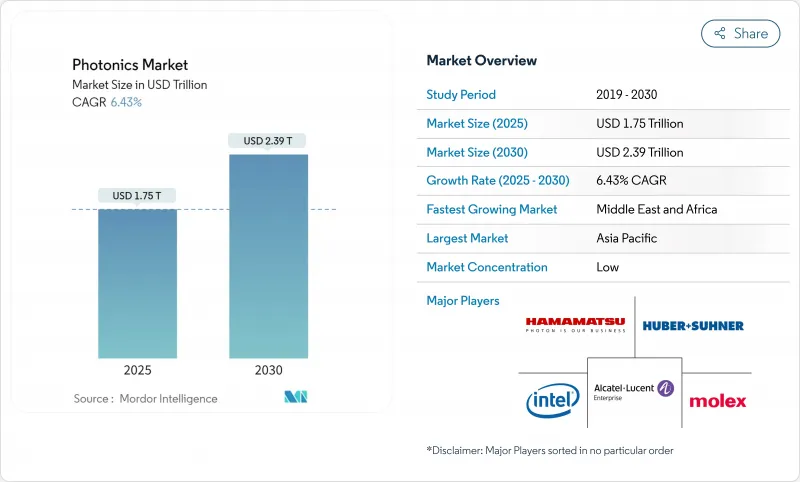
預計到 2025 年,光電市場規模將達到 1.75 兆美元,到 2030 年將達到 2.39 兆美元,複合年成長率為 6.43%。
資料中心內高速光鏈路的日益普及、汽車中雷射雷達(LiDAR)的滲透率不斷提高以及對節能型LED照明的持續需求,共同推動了光子學領域的擴張。印度的生產關聯激勵計畫(PLI)和歐盟的《晶片法案》等區域供應鏈計畫正在加速新建晶圓廠的建設,而矽光電新興企業的資金籌措也顯示了市場對晶片間光互連技術的信心。汽車原始設備製造商(OEM)正將雷射雷達作為高級駕駛輔助系統(ADAS)的標配,推動了光子學產品銷售的成長和成本的下降。同時,氮化鎵(GaN)和微型LED產能的提升也凸顯了市場正朝著降低消費和工業設備功耗的材料和裝置方向發展。
全球光電市場趨勢與洞察
資料中心互連的興起刺激了矽光電收發器的需求
人工智慧工作負載正在重塑超大規模資料中心,推動流量密度超越銅纜的承載極限。矽光電收發器的出貨速率現已超過 1.6 Tbps,在伺服器機架內擴展了傳輸距離,同時降低了每位元能耗。將光子層和電子層共封裝在 300 毫米晶圓上的代工平台,能夠增加光纖數量並降低耦合損耗,從而促進其在解耦架構中的應用。多輪融資,每輪均超過 1.5 億美元,印證了投資者對這一發展方向的信心。隨著營運商升級到光纖網路,調製器、加速器和整合雷射的量產也得到推動,進一步強化了光電市場的成長循環。
中國汽車OEM廠商採用以雷射雷達為基礎的ADAS系統
雷射雷達在價格分佈車型的快速普及正在重塑高級駕駛輔助系統(ADAS)的成本曲線。到2024年12月,中國領先的供應商每月將出貨超過10萬台車頂式雷射雷達,佔據全球33%的市場。與國內汽車製造商的夥伴關係正在拓展LiDAR的應用範圍,使其從高階SUV擴展到C級車,並推動零件標準化,從而縮短認證週期。政府支持的安全標準正在加速產品上市,並樹立了其他地區競相效仿的典範。
化合物半導體晶圓瓶頸限制了成長
InP 和 GaN基板的可得性落後於資料中心雷射和射頻功率元件的需求。少數幾家代工廠控制著 150 毫米以下尺寸的基板供應,這增加了地震或設備故障導致供應中斷的風險。雖然新的 CHIPS 法案資金正在支持德克薩斯州的產能擴張,但工具和製程的改進將前置作業時間延長至 2027 年,減緩了光電市場的成長勢頭。
細分市場分析
儘管基準,矽光電收發器預計仍將以 8.1% 的複合年成長率 (CAGR) 成為所有裝置類別中成長最快的。它們為伺服器、儲存和加速器架構提供動力,這些架構必須以每秒Petabyte級的速度傳輸資料。早期實現共封裝光元件的量產將降低每Gigabit位元的成本,並擴大其應用範圍。代工廠在電子層和光子層厚度同步方面的藍圖將增加設計庫,縮短原型製作時間,並使光電市場對雲端營運商更具吸引力。
LED在照明和背光領域佔據主導地位,預計到2024年將佔據光電市場32%的佔有率。新興的微型LED面板有望為電視、穿戴式裝置和汽車儀錶板帶來高亮度和長壽命。雷射二極體正在金屬切割和積層製造領域取得進展,而光學感測器則滿足了環境監測和智慧農業日益成長的需求。這些廣泛的應用領域使光電市場多元化,從而緩解了單一應用領域內的週期性波動。
到2024年,矽將佔據光電市場40.3%的佔有率,這得益於其成熟的設備和低成本的8吋晶圓。然而,氮化鎵(GaN)裝置預計將以9.3%的複合年成長率成長,在5G無線網路和電動車動力傳動系統所需的高頻率和高電壓下,GaN元件能夠實現更高的效率。歐洲一條200毫米GaN中試生產線以及美國聯邦政府提供的950萬美元製程開發津貼,正在推動該生態系統的發展。
玻璃、二氧化矽和聚合物平台擴展了光纖網路,並實現了靈活的成像陣列。 InP增益區和矽波導管的異質整合可製造出適用於共封裝光學元件的低成本雷射陣列。研究人員正在利用低損耗的SiN層來擴展頻譜覆蓋範圍,而聚合物在生物感測一次性拋棄式領域也越來越受歡迎。這種材料的多樣性確保了光電市場始終以創新主導,而不會局限於單一基板。
產業領導者正在推行規模化和專業化擴大策略。 LED製造商將外延和封裝生產線集中佈局,以縮短物流時間;而收發器新興企業則透過授權製程設計套件來利用現有代工廠的資源。企業併購,例如以7.285億美元收購模組製造商,反映出市場對承包光連接產品組合的需求。組件製造商的藍圖越來越強調電子和光學元件的協同最佳化,凸顯了融合設計架構將如何推動光電市場的發展。
不同基板的供應動態各不相同。矽晶圓的供應鏈充足,而半絕緣氮化鎵基板的合格供應商數量較少,導致前置作業時間不穩定。平台融合正逐漸成為一種對沖策略。整合設備製造商可利用現有工具集,將晶粒晶片鍵結到矽載體上,或在QST1模板上沉積氮化鎵。這些混合堆疊結構降低了每瓦光功率的資本支出,增強了光電市場的韌性。
區域分析
亞太地區,在中國大陸、台灣、日本和韓國等半導體產業叢集的驅動下,將引領光電市場,預計到2024年將佔45.7%的營收佔有率。中國本土LiDAR(LiDAR)領軍企業將佔據全球33%的銷售佔有率,預計2024年出貨量將超過150萬台,凸顯其強大的本土化規模生產能力。台灣的晶圓代工生態系統正在引領光電和電子學一體化平台的建設,確保關鍵智慧財產權即使在2025年2月地震導致工廠生產中斷後仍能留在該地區。日本的玻璃和精密光學公司正在供應特殊基板,而韓國的顯示器製造商正在擴大微型LED試點生產線。
北美在研發支出方面保持著較高的佔有率。 2025年2月,一家光連接模組新興企業獲得1.75億美元的創業投資資金,凸顯了投資者對能夠降低資料中心能耗的硬體的濃厚興趣。根據《晶片法案》(CHIPS Act),聯邦政府的激勵措施正將資金投入到磷化銦(InP)和矽磷化矽(SiPh)的試點生產線,從而拓展了國內光電領域的選擇,使其不再局限於國防領域。歐洲正利用綠色交易」和《歐洲晶片法案》,在義大利建造一座價值20億歐元的碳化矽(SiC)和氮化鎵(GaN)巨型工廠,目標是到2030年將其製造業佔有率翻倍。
中東和非洲將以7.2%的複合年成長率實現最快的成長,這主要得益於光纖骨幹網部署和太陽能發電廠監測的需求。南美經濟體正在投資精密農業感測技術,該技術依賴本地組裝的高光譜遙測成像器。在所有地區,微影術工具的貿易限制正在改變資本投資的時機。供應商正在透過採取雙源策略來應對,從而保持光電市場的韌性。
其他福利:
- Excel格式的市場預測(ME)表
- 3個月的分析師支持
目錄
第1章 引言
- 研究假設和市場定義
- 調查範圍
第2章調查方法
第3章執行摘要
第4章 市場情勢
- 市場概覽
- 市場促進因素
- 資料中心互連的成長推動了北美對矽光電收發器的需求
- 中國汽車OEM廠商採用以雷射雷達為基礎的ADAS系統
- 歐盟綠色交易對微型LED和GaN晶圓廠的獎勵
- 印度的生產關聯激勵計劃促進了國內光電叢集的發展
- 美國和歐洲照護現場感測技術蓬勃發展
- 太空衛星衛星群星座投資-合格光電
- 市場限制
- 化合物半導體晶圓(InP、GaN,小於150毫米)的瓶頸
- 功率超過 10kW 的二極體雷射的溫度控管限制
- 整合光學積體電路標準之間的互通性差距
- 中美貿易限制增加了工具製造商的資本投資風險
- 產業生態系分析
- 技術展望
- 波特五力分析
- 供應商的議價能力
- 買方的議價能力
- 新進入者的威脅
- 替代品的威脅
- 競爭對手之間的競爭
第5章 市場規模與成長預測
- 依產品
- 雷射
- 二極體雷射
- 光纖雷射
- 固態及其他
- LED
- 感測器和檢測器
- 光纖和波導
- 調製器和開關
- 其他
- 雷射
- 材料
- 矽
- 玻璃和二氧化矽
- 化合物半導體(InP、GaAs、GaN)
- 聚合物和塑膠
- 其他
- 波長
- 紫外線 (UV)
- 可見的
- 紅外線的
- 按最終用戶行業分類
- 消費性電子產品
- 航太與國防
- 顯示與成像
- 太陽能發電
- LED照明
- 醫療器材和生物設備
- 工業和製造業
- 汽車(包括LiDAR)
- 數據與通訊
- 其他
- 按地區
- 北美洲
- 美國
- 加拿大
- 墨西哥
- 歐洲
- 德國
- 英國
- 法國
- 義大利
- 西班牙
- 其他歐洲地區
- 亞太地區
- 中國
- 日本
- 韓國
- 印度
- 東南亞
- 亞太其他地區
- 南美洲
- 巴西
- 其他南美洲
- 中東和非洲
- 中東
- 阿拉伯聯合大公國
- 沙烏地阿拉伯
- 其他中東地區
- 非洲
- 南非
- 其他非洲地區
- 北美洲
第6章 競爭情勢
- 市場集中度
- 策略趨勢
- 市佔率分析
- 公司簡介
- Hamamatsu Photonics KK
- Intel Corporation
- Nokia Corporation(Alcatel-Lucent)
- Coherent Corp.
- AMS OSRAM AG
- IPG Photonics Corp.
- Signify NV
- Lumentum Holdings Inc.
- Infinera Corp.
- NEC Corp.
- Corning Inc.
- Schott AG
- Thorlabs Inc.
- Jenoptik AG
- Trumpf Photonics GmbH
- Molex LLC
- Rockley Photonics Ltd.
- Innolume GmbH
- Aeva Technologies Inc.
- Broadcom Inc.(Silicon Photonics)
- Carl Zeiss AG(incl. Scantinel)
- Nikon Corp.
第7章 市場機會與未來展望
The photonics market is valued at USD 1.75 trillion in 2025 and is set to advance to USD 2.39 trillion by 2030 at a 6.43% CAGR.
Expansion rests on the rising deployment of high-speed optical links inside data centers, growing LiDAR penetration in vehicles and sustained demand for energy-efficient LED lighting. Regional supply-chain programs, such as India's PLI scheme and the EU Chips Act, are accelerating new fab construction, while corporate funding rounds for silicon-photonics start-ups signal confidence in chip-to-chip optical interconnects. Automotive OEMs are standardizing LiDAR as an ADAS staple, stimulating volume growth and cost declines. At the same time, GaN and micro-LED capacity ramp-ups underline the shift toward materials and devices that lower power budgets in consumer and industrial equipment.
Global Photonics Market Trends and Insights
Proliferation of data-center interconnect spurring silicon photonics transceiver demand
AI workloads are restructuring hyperscale data centers, pushing traffic density beyond copper's limits. Silicon photonics transceivers now ship with data-rates above 1.6 Tbps, cutting energy per bit while lengthening reach inside server racks. Foundry platforms that co-package photonic and electronic layers on 300 mm wafers allow high fiber counts and lower coupling loss, which eases adoption in disaggregated architectures. Multiple venture rounds exceeding USD 150 million each underscore investor conviction in this path. As operators upgrade to optical fabrics, they also stimulate volume production of modulators, drivers and integrated lasers, reinforcing the photonics market growth loop.
Adoption of LiDAR-based ADAS across Chinese automotive OEMs
Rapid LiDAR integration in mid-price vehicles is redefining ADAS cost curves. A leading Chinese supplier shipped more than 100,000 roof-mounted units monthly by December 2024, capturing 33% global share.Partnerships with domestic OEMs extend LiDAR coverage from premium SUVs to C-segment cars, triggering component standardization that shortens qualification cycles. Government-supported safety standards are accelerating time-to-market, creating a template other regions are starting to emulate.
Compound-semiconductor wafer bottlenecks constraining growth
InP and GaN substrate availability lags demand from data-center lasers and RF power devices. A handful of foundries control sub-150 mm supply, heightening disruption risks when earthquakes or equipment faults occur. While new CHIPS Act funding backs capacity expansions in Texas, tools and process qualifications stretch lead times into 2027, slowing the photonics market momentum.
Other drivers and restraints analyzed in the detailed report include:
- EU Green-Deal incentives for micro-LED and GaN photonics fabs
- India's PLI scheme catalyzing domestic photonics clusters
- Thermal-management limits hampering high-power laser development
For complete list of drivers and restraints, kindly check the Table Of Contents.
Segment Analysis
Silicon photonics transceivers hold a modest baseline but are forecast to expand at an 8.1% CAGR, the highest among device classes. They underpin server, storage and accelerator fabrics that must move petabytes every second. Early volume ramps in co-packaged optics bring down dollar-per-gigabit metrics, widening the adoption window. As foundry roadmaps sync electronic and photonic layer thicknesses, design libraries grow and time-to-prototype shortens, elevating the photonics market appeal for cloud operators.
LEDs, with 32% of 2024 photonics market share, dominate lighting and backlighting. Emerging micro-LED panels promise higher brightness and longer life for televisions, wearables and automotive clusters. Laser diodes penetrate metal cutting and additive manufacturing, while optical sensors tag rising demand for environmental monitoring and smart agriculture. The breadth of these categories keeps the photonics market diversified, cushioning cyclic swings in any single application group.
Silicon still accounts for 40.3% of the photonics market size in 2024, benefiting from mature equipment sets and low-cost eight-inch wafers. However, GaN devices, forecast to grow at 9.3% CAGR, attain higher efficiency at elevated frequencies and voltages, key for 5G radios and electric-vehicle powertrains. Subsidized 200 mm GaN pilot lines in Europe and US federal grants of USD 9.5 million for process development encourage ecosystem growth.
Glass, silica and polymer platforms expand fiber networks and enable flexible imaging arrays. Heterogeneous integration of InP gain sections with silicon waveguides produces low-cost laser arrays suited for co-packaged optics. Researchers exploit low-loss SiN layers to broaden spectral coverage, while polymers gain traction in biosensing disposables. Such material diversity ensures that the photonics market remains innovation-driven rather than locked to a single substrate.
Segment leaders pursue scale or specialization strategies. LED manufacturers co-locate epitaxy and packaging lines to cut logistics time, whereas transceiver start-ups license process design kits to tap established foundries. Corporate M&A, such as a USD 728.5 million module-maker acquisition, reflects the need for turnkey optical-connect portfolios. Component-maker roadmaps increasingly list co-optimization of electronics and optics, underscoring how converged design stacks propel the photonics market forward.
Supply dynamics vary by substrate. Silicon wafers draw on an abundant supply chain, whereas semi-insulating GaN substrates rely on fewer qualified suppliers, amplifying lead-time volatility. Platform convergence emerges as a hedge: integrated device manufacturers bond GaN dies on silicon carriers or deposit GaN on QST1 templates to benefit from existing toolsets. These hybrid stacks lower capex per watt of optical output, reinforcing the photonics market resilience.
The Photonics Market Report is Segmented by Product (Lasers, Leds, Sensors and Detectors, and More), Material (Silicon, Glass and Silica, and More), Wavelength (Ultraviolet, Visible, and Infrared), End-User Industry (Consumer Electronics, Aerospace and Defense, Display and Imaging, Solar Photovoltaics, LED Lighting, Medical and Bio-Instrumentation, and More), and Geography. The Market Forecasts are Provided in Terms of Value (USD).
Geography Analysis
Asia-Pacific led the photonics market with a 45.7% revenue share in 2024, fueled by semiconductor clusters in China, Taiwan, Japan and South Korea. China's domestic LiDAR champion recorded 33% global volume share and shipped more than 1.5 million units in 2024, underscoring local capacity to scale. Taiwan's foundry ecosystem pioneers integrated photonic-electronic platforms, ensuring that critical IP stays within regional boundaries even after the February 2025 earthquake disrupted fab output. Japan's glass and precision optics firms supply specialty substrates, while South Korean display makers expand micro-LED pilot lines.
North America maintains a high share of R&D expenditure. Venture funding of USD 175 million for an optical interconnect start-up in February 2025 highlighted investor appetite for hardware that cuts data-center power. Federal incentives under the CHIPS Act channel money toward InP and SiPh pilot lines, broadening domestic options beyond defense-specific photonics. Europe leverages the Green Deal and the European Chips Act to double manufacturing share by 2030, with a EUR 2 billion SiC and GaN megaplant in Italy among the flagship projects.
The Middle East and Africa post the fastest CAGR at 7.2%, driven by optical-fiber backbone rollouts and solar-farm monitoring needs. South American economies invest in precision-agriculture sensing that relies on hyperspectral imagers assembled locally. Across all regions, trade restrictions on lithography tools reshape capex timing. Suppliers respond by pursuing dual-source strategies, thereby preserving resilience in the photonics market.
- Hamamatsu Photonics KK
- Intel Corporation
- Nokia Corporation (Alcatel-Lucent)
- Coherent Corp.
- AMS OSRAM AG
- IPG Photonics Corp.
- Signify NV
- Lumentum Holdings Inc.
- Infinera Corp.
- NEC Corp.
- Corning Inc.
- Schott AG
- Thorlabs Inc.
- Jenoptik AG
- Trumpf Photonics GmbH
- Molex LLC
- Rockley Photonics Ltd.
- Innolume GmbH
- Aeva Technologies Inc.
- Broadcom Inc. (Silicon Photonics)
- Carl Zeiss AG (incl. Scantinel)
- Nikon Corp.
Additional Benefits:
- The market estimate (ME) sheet in Excel format
- 3 months of analyst support
TABLE OF CONTENTS
1 INTRODUCTION
- 1.1 Study Assumptions and Market Definition
- 1.2 Scope of the Study
2 RESEARCH METHODOLOGY
3 EXECUTIVE SUMMARY
4 MARKET LANDSCAPE
- 4.1 Market Overview
- 4.2 Market Drivers
- 4.2.1 Proliferation of data-center interconnect spurring silicon photonics transceiver demand in North America
- 4.2.2 Adoption of LiDAR-based ADAS across Chinese automotive OEMs
- 4.2.3 EU Green-Deal incentives for micro-LED and GaN photonics fabs
- 4.2.4 India's PLI scheme catalyzing domestic photonics clusters
- 4.2.5 Point-of-care biosensing surge in United States and Europe
- 4.2.6 Satellite mega-constellation investments in space-qualified photonics
- 4.3 Market Restraints
- 4.3.1 Compound-semiconductor wafer bottlenecks (InP, GaN <150 mm)
- 4.3.2 Thermal-management limits on >10 kW diode lasers
- 4.3.3 Interoperability gaps among integrated photonic IC standards
- 4.3.4 U.S.-China trade controls elevating cap-ex risk for tool makers
- 4.4 Industry Ecosystem Analysis
- 4.5 Technological Outlook
- 4.6 Porter's Five Forces Analysis
- 4.6.1 Bargaining Power of Suppliers
- 4.6.2 Bargaining Power of Buyers
- 4.6.3 Threat of New Entrants
- 4.6.4 Threat of Substitutes
- 4.6.5 Intensity of Competitive Rivalry
5 MARKET SIZE AND GROWTH FORECASTS (VALUES)
- 5.1 By Product
- 5.1.1 Lasers
- 5.1.1.1 Diode Lasers
- 5.1.1.2 Fiber Lasers
- 5.1.1.3 Solid-state and Others
- 5.1.2 LEDs
- 5.1.3 Sensors and Detectors
- 5.1.4 Optical Fibers and Waveguides
- 5.1.5 Modulators and Switches
- 5.1.6 Others
- 5.1.1 Lasers
- 5.2 By Material
- 5.2.1 Silicon
- 5.2.2 Glass and Silica
- 5.2.3 Compound Semiconductors (InP, GaAs, GaN)
- 5.2.4 Polymers and Plastics
- 5.2.5 Others
- 5.3 By Wavelength
- 5.3.1 Ultraviolet (UV)
- 5.3.2 Visible
- 5.3.3 Infrared
- 5.4 By End-user Industry
- 5.4.1 Consumer Electronics
- 5.4.2 Aerospace and Defense
- 5.4.3 Display and Imaging
- 5.4.4 Solar Photovoltaics
- 5.4.5 LED Lighting
- 5.4.6 Medical and Bio-instrumentation
- 5.4.7 Industrial and Manufacturing
- 5.4.8 Automotive (incl. LiDAR)
- 5.4.9 Data and Telecom
- 5.4.10 Others
- 5.5 By Geography
- 5.5.1 North America
- 5.5.1.1 United States
- 5.5.1.2 Canada
- 5.5.1.3 Mexico
- 5.5.2 Europe
- 5.5.2.1 Germany
- 5.5.2.2 United Kingdom
- 5.5.2.3 France
- 5.5.2.4 Italy
- 5.5.2.5 Spain
- 5.5.2.6 Rest of Europe
- 5.5.3 Asia-Pacific
- 5.5.3.1 China
- 5.5.3.2 Japan
- 5.5.3.3 South Korea
- 5.5.3.4 India
- 5.5.3.5 South East Asia
- 5.5.3.6 Rest of Asia-Pacific
- 5.5.4 South America
- 5.5.4.1 Brazil
- 5.5.4.2 Rest of South America
- 5.5.5 Middle East and Africa
- 5.5.5.1 Middle East
- 5.5.5.1.1 United Arab Emirates
- 5.5.5.1.2 Saudi Arabia
- 5.5.5.1.3 Rest of Middle East
- 5.5.5.2 Africa
- 5.5.5.2.1 South Africa
- 5.5.5.2.2 Rest of Africa
- 5.5.1 North America
6 COMPETITIVE LANDSCAPE
- 6.1 Market Concentration
- 6.2 Strategic Moves
- 6.3 Market Share Analysis
- 6.4 Company Profiles {(includes Global level Overview, Market level overview, Core Segments, Financials as available, Strategic Information, Market Rank/Share for key companies, Products and Services, and Recent Developments)}
- 6.4.1 Hamamatsu Photonics KK
- 6.4.2 Intel Corporation
- 6.4.3 Nokia Corporation (Alcatel-Lucent)
- 6.4.4 Coherent Corp.
- 6.4.5 AMS OSRAM AG
- 6.4.6 IPG Photonics Corp.
- 6.4.7 Signify NV
- 6.4.8 Lumentum Holdings Inc.
- 6.4.9 Infinera Corp.
- 6.4.10 NEC Corp.
- 6.4.11 Corning Inc.
- 6.4.12 Schott AG
- 6.4.13 Thorlabs Inc.
- 6.4.14 Jenoptik AG
- 6.4.15 Trumpf Photonics GmbH
- 6.4.16 Molex LLC
- 6.4.17 Rockley Photonics Ltd.
- 6.4.18 Innolume GmbH
- 6.4.19 Aeva Technologies Inc.
- 6.4.20 Broadcom Inc. (Silicon Photonics)
- 6.4.21 Carl Zeiss AG (incl. Scantinel)
- 6.4.22 Nikon Corp.
7 MARKET OPPORTUNITIES AND FUTURE OUTLOOK
- 7.1 White-space and Unmet-need Assessment
 2026年全球光電市場報告
 先進光電市場預測至2034年—按產品、技術、應用、最終用戶和地區分類的全球分析
 光電研究評論:2025
 光電市場報告:按類型、應用、最終用戶和地區分類(2026-2034 年)
 光電市場:按產品類型、技術和應用分類的全球市場預測 - 2026-2032 年
 光電晶片市場分析及預測(至2035年):類型、產品類型、技術、組件、應用、材料類型、裝置、最終用戶、功能
 光子學市場:依產品類型、應用和終端用戶產業劃分 - 至2036年的全球預測光電市場分析及預測(至2035年):依類型、產品類型、服務、技術、組件、應用、材料類型、裝置、最終用戶、功能分類
 美國光電:市場佔有率分析、行業趨勢和統計數據、成長預測(2026-2031)
 光電市場-全球產業規模、佔有率、趨勢、機會及預測(依產品類型、應用、最終用戶、地區及競爭格局分類,2021-2031年)