


 |
市場調查報告書
商品編碼
1844674
奈米輻射感測器:市場佔有率分析、行業趨勢、統計數據和成長預測(2025-2030)Nano Radiation Sensors - Market Share Analysis, Industry Trends & Statistics, Growth Forecasts (2025 - 2030) |
||||||
※ 本網頁內容可能與最新版本有所差異。詳細情況請與我們聯繫。
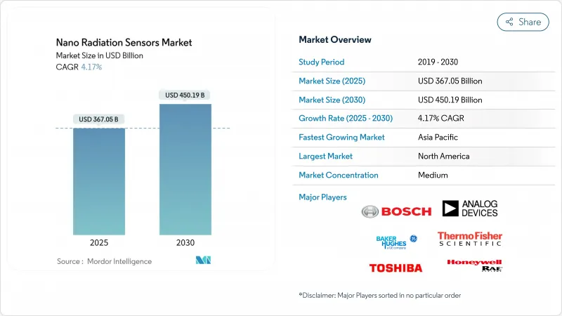
預計到 2025 年奈米輻射感測器市場規模將達到 3,670.5 億美元,複合年成長率為 4.17%,到 2030 年將達到 4,501.9 億美元。
成長反映了家用電子電器、航太和汽車系統的持續小型化,以及核能發電廠退役和太空探索方面嚴格的安全法規。鈣鈦礦半導體材料的最新突破使檢測器的佔地面積足夠小,可以整合智慧型手機和穿戴式貼片,消除了長期存在的尺寸和功率障礙。政府獎勵策略,從英國核能退役管理局提供的 3000 萬英鎊一攬子計劃到為 ADI 公司提供的 1.05 億美元 CHIPS 法案撥款,正在縮短商業化週期並加速供應擴張。立方衛星的激增,特別是在大學和新興企業任務中的激增,增加了超輕型感測器的可尋址容量,同時醫療劑量測定和汽車安全子系統的需求也在增加。雖然製造複雜性和產量比率下降仍然是最顯著的限制因素,但能夠解決材料穩定性問題同時保持成本控制的公司將獲得直接的競爭優勢。
全球奈米輻射感測器市場趨勢與洞察
各行業的裁員趨勢
消費性電子產品和汽車平台的持續小型化推動了輻射感測器模組在晶圓級的整合。夏普展示了一款25 x 20 x 2.5毫米的模組,功耗僅7.5毫瓦,使智慧型手機中的輻射追蹤實用化成為可能。 5奈米和3奈米製程節點的平行發展使邏輯電路和檢測電路共用通用晶粒,從而降低了目標商標產品製造商的物料清單成本。在汽車領域,微型感測器現在可以安裝在現有的電控系統內,因此無需改變駕駛室設計即可支援高級駕駛輔助系統(ADAS)。隨著物聯網架構的日益普及,分散式奈米輻射感測器可以以五年前無法企及的節點級成本部署在工廠和醫院。
政府奈米技術資金和標準
有針對性的公共計畫確保了長期需求,同時協調了認證。美國商務部向ADI公司撥款1.05億美元,用於其三家國內工廠的現代化改造。英國核能退役管理局已承諾投入3,000萬英鎊用於感測器研發,以支持老舊核子反應爐的安全退役。同時,歐盟委員會的「地平線歐洲」平台正將資源投入永續輻射防護技術。 ISO和IEEE工作小組目前正在起草統一的奈米感測器測試通訊協定,以縮短合規週期並實現跨境採購。
製造複雜性和產量比率損失
先進檢測器架構所需的10奈米以下製程的缺陷率高於主流邏輯晶片,導致一些代工廠的一次通過產量比率低於60%。供應鏈衝擊,例如為光刻光罩基板提供高純度二氧化矽的Spruce Pine石英礦的暫時關閉,透過限制關鍵材料供應,加劇了成本壓力。晶圓廠營運商不得不採用更嚴格的顆粒控制和先進的計量技術,從而在短期內推高了每片晶圓的營運成本。
細分分析
固體檢測器利用CMOS相容性將感測元件直接整合到混合訊號晶片上,到2024年將佔奈米輻射感測器市場收入的58%。這種架構在醫學成像和衛星設備中很受歡迎,因為它可以降低功耗並簡化基板佈局。閃爍單元雖然市佔率較小,但由於鈣鈦礦奈米晶體的突破,其光輸出已超過100,000 MeV-1,因此正受惠於6.5%的複合年成長率。將固體讀出與奈米晶體閃爍體結合的混合設計現已實現低於400 ps的響應速度,同時保持了晶圓級加工的經濟性。
第二代固體平台採用奈米等離子體增強層,在不增加佔地面積的情況下將光子收集效率提高了三倍。隨著鈣鈦礦塗層的成熟,製造商正在嘗試將高Z閃爍體單晶片整合到矽光電二極體上,旨在打造用於內視鏡手術的單晶片伽馬攝影機。這一發展表明固體方法和閃爍方法之間的界限正在模糊,為整個奈米輻射感測器產業創造了新的收益來源。
到2024年,矽材料將維持46%的收入貢獻,透過提供可靠的供應和廣泛的代工支持,支撐當前主流應用的奈米輻射感測器市場規模。良好的生產學習曲線使平均售價保持可預測性,這對於致力於十年產品週期的一級汽車供應商至關重要。鈣鈦礦檢測器的複合年成長率為8.2%,得益於能夠實現軟式電路板捲對輥塗的溶液處理技術,從而拓展了穿戴式健康監測器和無人機平台的應用機會。
將矽基ASIC與薄鈣鈦礦吸收層結合的複合堆疊,能夠在單一封裝內偵測軟X光和低能量伽瑪光子,從而改善無損檢測的頻譜成像。以錳錯合為特徵的無鉛組合物可提供超過80%的光致發光量子產率,在不犧牲檢測效率的情況下實現環境升級。這些混合堆疊代表著曲折點,材料選擇決策將不再受供應鏈約束,而是取決於具體應用。
奈米輻射感測器市場按類型(閃爍檢測器、固體檢測器)、材料(矽基半導體、無機晶體(GAGG、LSO、Csi)等)、應用(汽車、消費性電子等)、技術(間接閃爍 - CMOS 等)、探測輻射類型、外形尺寸和地區細分。市場預測以美元計算。
區域分析
北美的領先地位將在2024年達到35%的佔有率,這得益於持續的國防採購和耗資數十億美元對93座運作中的核子反應爐進行現代化升級。 ADI公司正在根據《晶片法案》(CHIPS Act)將其在馬薩諸塞州和奧勒岡州的晶圓產量增加兩倍,以確保軍用級檢測器的長期供應。賽默飛世爾科技正在擴大其在美國的64個製造地網路,以加強醫療保健、工業無損檢測和國防安全保障項目的國內供應,同時提供人工智慧驅動的監控和預測分析,以減少美國兩座壓水式反應爐的計劃外停機時間。
受中國智慧型手機相容輻射晶片成功推廣的推動,亞太地區將以5.9%的複合年成長率位居榜首。日本憑藉夏普的超薄感測器模組和日本原子能機構(JAEA)用於沸水式反應爐維修的矽伽馬射線檢測器,保持了其在核領域的專業優勢。韓國NEXTSat-2衛星上的LEO-DOS有效載荷將檢驗其自主研發的低軌道劑量抗輻射設計,並向東南亞新興航太經濟體展示可出口的潛力。
在歐洲,安全退役171吉瓦的核能發電廠,這些核電廠將於2050年前逐步淘汰,這將在短期內導致分散式感測器陣列的需求達到高峰。英國將撥款3000萬英鎊津貼一個產學研聯盟,開發自主機器人監測器的原型。一家德國一級汽車供應商正在考慮將輻射感測技術納入ADAS控制單元,以確保電子設備免受單粒子故障的影響;法國電力公司(EDF)正在使用奈米感測器升級堆芯通量測繪技術,以將核電站許可證的有效期延長至60年或更長時間。芬蘭於韋斯屈萊大學開發了一種手持式多用途檢測器,它結合了中子、伽馬射線和BETA射線,為芬蘭各地的初期應變人員套件提供支援。
其他福利:
- Excel 格式的市場預測 (ME) 表
- 3個月的分析師支持
目錄
第1章 引言
- 研究假設和市場定義
- 調查範圍
第2章調查方法
第3章執行摘要
第4章 市場狀況
- 市場概況
- 市場促進因素
- 整個產業都朝著小型化發展
- 政府奈米技術資助和標準化
- 高精度醫療劑量計的需求不斷增加
- 核能退役和安全法規
- 立方衛星和小型衛星採用奈米感測器
- 使用軟性鈣鈦礦閃爍體的穿戴式劑量測定
- 市場限制
- 製造複雜性和產量比率損失
- 奈米製造生產線的資本成本高昂
- 原始設備製造商之間缺乏整合標準
- 鈣鈦礦/有機材料的穩定性問題
- 價值/供應鏈分析
- 監管狀況
- 技術展望
- 關鍵績效指標(KPI)
- 波特五力分析
- 新進入者的威脅
- 買方的議價能力
- 供應商的議價能力
- 替代品的威脅
- 競爭對手之間的競爭強度
第5章市場規模及成長預測
- 按類型
- 閃爍檢測器
- 固體檢測器
- 按材質
- 矽基半導體
- 無機晶體(GAGG、LSO、CsI)
- 鈣鈦礦半導體(含鉛和無鉛)
- 有機/聚合物閃爍體
- 按用途
- 車
- 消費性電子產品
- 衛生保健
- 產業
- 石油和天然氣
- 發電
- 其他用途
- 依技術
- 直接轉換(光子計數)
- 間接閃爍-CMOS
- 軟性/穿戴面板
- 抗輻射SoC和SiPM
- 根據偵測到的輻射類型
- 阿爾法
- BETA射線
- 伽瑪射線/X光
- 中子
- 外形規格
- 晶片級
- 模組
- 控制板
- 穿戴式貼片
- 按地區
- 北美洲
- 美國
- 加拿大
- 墨西哥
- 南美洲
- 巴西
- 阿根廷
- 其他南美
- 歐洲
- 英國
- 德國
- 法國
- 義大利
- 俄羅斯
- 西班牙
- 其他歐洲國家
- 亞太地區
- 中國
- 日本
- 印度
- 韓國
- 其他亞太地區
- 中東和非洲
- 中東
- 阿拉伯聯合大公國
- 沙烏地阿拉伯
- 土耳其
- 其他中東地區
- 非洲
- 南非
- 埃及
- 其他非洲國家
- 北美洲
第6章 競爭態勢
- 市場集中度
- 策略舉措
- 市佔率分析
- 公司簡介
- Analog Devices Inc.
- Robert Bosch GmbH
- Nihon Kessho Kogaku Co. Ltd.
- Thermo Fisher Scientific Inc.
- Baker Hughes Co.
- Honeywell International Inc.(RAE Systems)
- First Sensor AG(TE Connectivity)
- Hamamatsu Photonics KK
- Toshiba Corporation
- Mirion Technologies Inc.
- Fortive Corporation
- PerkinElmer Inc.(Revvity)
- Radiation Monitoring Devices Inc.
- Texas Instruments Inc.
- Lockheed Martin Corp.
- OMRON Corporation
- Space Micro Inc.
- Analogic Corporation
- Canon Medical Systems Corp.
- Siemens Healthineers AG
- GE Healthcare Technologies Inc.
- BAE Systems plc
- Hitachi Ltd.
- STMicroelectronics NV
第7章 市場機會與未來展望
The nano radiation sensors market stood at USD 367.05 billion in 2025 and is forecast to register a 4.17% CAGR, reaching USD 450.19 billion by 2030.
Growth reflects consistent miniaturization across consumer electronics, aerospace, and automotive systems, paired with stringent safety rules in nuclear decommissioning and space exploration. Recent breakthroughs in perovskite semiconductor materials now allow detector footprints small enough for smartphone integration and wearable patches, removing long-standing size and power barriers. Government stimulus ranging from the GBP 30 million package under the UK Nuclear Decommissioning Authority to the USD 105 million CHIPS Act grant for Analog Devices shortens commercialization cycles and accelerates supply expansion. CubeSat proliferation, particularly in university and startup missions, compounds the addressable volume for ultra-light sensors, while parallel demand arises from healthcare dosimetry and automotive safety subsystems. Manufacturing complexity and yield losses remain the most significant constraints; however, firms that resolve material-stability issues while maintaining cost control gain an immediate competitive edge.
Global Nano Radiation Sensors Market Trends and Insights
Miniaturization trend across industries
Relentless downsizing in consumer electronics and automotive platforms pushes radiation sensor modules toward wafer-level integration. Sharp demonstrated a 25 X 20 X 2.5 mm module drawing only 7.5 mW, making smartphone-based radiation tracking practical. Parallel progress in 5 nm and 3 nm process nodes allows logic and detection circuitry to share a common die, lowering bill-of-materials costs for original-equipment manufacturers. In automobiles, compact sensors now fit inside existing electronic control units, supporting Advanced Driver Assistance Systems without altering cabin design. As IoT architectures spread, distributed nano radiation sensors can be deployed in factories and hospitals at node-level costs that were unattainable five years ago.
Government nanotech funding and standards
Targeted public programs guarantee long-term demand while harmonizing certification. The U.S. Department of Commerce earmarked USD 105 million for Analog Devices to modernize three domestic fabs, explicitly citing commercial and defense radiation detection as priority outputs. The UK Nuclear Decommissioning Authority injected GBP 30 million into sensor R & D to support safe dismantling of legacy reactors. In parallel, the European Commission's Horizon Europe platform directs resources toward sustainable radiation-protection technology. ISO and IEEE working groups now draft unified nano sensor test protocols that cut compliance cycles and enable cross-border procurement.
Manufacturing complexity and yield losses
Sub-10 nm features needed for latest detector architectures experience higher defect rates than mainstream logic chips, depressing first-pass yields below 60% at several foundries. Supply-chain shocks-such as the temporary shutdown of Spruce Pine's quartz mine that feeds high-purity silica into photolithography mask blanks-amplify cost pressures by constricting vital materials. Fab operators must adopt tighter particulate controls and advanced metrology, driving up per-wafer operating expenses in the short run.
Other drivers and restraints analyzed in the detailed report include:
- Growing demand for high-precision healthcare dosimetry
- Nuclear decommissioning and safety regulations
- Stability issues of perovskite / organic materials
For complete list of drivers and restraints, kindly check the Table Of Contents.
Segment Analysis
Solid-state detectors captured 58% of 2024 revenue within the nano radiation sensors market, leveraging CMOS compatibility to embed sensing elements directly onto mixed-signal chips. This architecture trims power budgets and simplifies board layouts, attributes valued in medical imaging consoles and satellite payloads. Scintillation units, though smaller in share, benefit from 6.5% CAGR prospects tied to perovskite nanocrystal breakthroughs delivering light yields above 100,000 photons MeV-1. Hybrid designs now merge solid-state readout with nanocrystal scintillators, achieving sub-400 ps response while retaining wafer-level processing economies.
Second-generation solid-state platforms adopt nano-plasmonic enhancement layers that triple photon-collection efficiency without expanding footprint. As perovskite coatings mature, manufacturers experiment with monolithic integration of high-Z scintillators atop silicon photodiodes, pointing toward single-chip gamma cameras for endoscopic surgery. The evolution indicates that categorical boundaries between solid-state and scintillation approaches will blur, generating new revenue pools throughout the nano radiation sensors industry.
Silicon maintained 46% contribution to 2024 revenue, offering reliable supply and extensive foundry support that underpins the current nano radiation sensors market size for mainstream applications. Production learning curves keep average selling prices predictable, a trait essential for automotive Tier-1 suppliers committing to decade-long product cycles. Perovskite detectors, at 8.2% CAGR, benefit from solution processing that allows roll-to-roll coating of flexible substrates, widening addressable opportunities in wearable health monitors and drone platforms.
Composite stacks merging silicon ASICs with thin perovskite absorber layers allow detection of soft X-ray and low-energy gamma photons in a single envelope, improving multispectral imaging for nondestructive testing. Lead-free compositions featuring manganese complexes reach photoluminescence quantum yields above 80%, providing an environmental upgrade without sacrificing detection efficiency. These hybrid stacks signal an inflection point where material-choice decisions become application-specific rather than supply-chain constrained.
Nano Radiation Sensors Market Segmented by Type (Scintillation Detectors, Solid-State Detectors), Material (Silicon-Based Semiconductors, Inorganic Crystals (GAGG, LSO, Csi) and More), Application (Automotive, Consumer Electronics and More), Technology, Indirect Scintillation-CMOS and More), Detection Radiation Type, Form Factor and Geography. The Market Forecasts are Provided in Terms of Value (USD).
Geography Analysis
North American leadership, with 35% 2024 share, is anchored by continuous defense procurement and multi-billion-dollar modernization across 93 operating nuclear reactors. Analog Devices is tripling wafer starts in Massachusetts and Oregon under the CHIPS Act, securing long-run availability of military-grade detectors. Thermo Fisher's enlarged US network of 64 manufacturing sites reinforces domestic supply for healthcare, industrial NDT, and homeland-security programs, while AI-augmented monitoring at two US pressurized-water reactors cuts unscheduled outage hours through predictive analytics.
APAC shows the fastest 5.9% CAGR forecast, underpinned by China's successful scaling of smartphone-compatible radiation chips, which broaden public-safety adoption. Japan maintains domain expertise via Sharp's ultra-thin sensor module and JAEA's silicon gamma-ray detectors qualified for boiling-water reactor retrofits. South Korea's LEO-DOS payload on NEXTSat-2 validates homegrown radiation-hard designs for low-Earth-orbit dosimetry, signalling export-ready competence for emerging space economies in Southeast Asia.
Europe prioritizes safe dismantling of 171 GW of nuclear capacity set for phase-out before 2050, creating near-term demand peaks for distributed sensor arrays. The UK's GBP 30 million research grant seeds university-industry consortia to prototype autonomous robotic monitors. Germany's automotive Tier-1 suppliers explore integrating radiation sensing into ADAS control units to certify electronics against single-event upsets, while France's EDF upgrades core flux mapping with nano sensors to extend plant licenses beyond 60 years. Finland's University of Jyvaskyla produced a handheld multi-purpose detector that merges neutron, gamma, and beta channels, supporting first-responder toolkits across the continent.
- Analog Devices Inc.
- Robert Bosch GmbH
- Nihon Kessho Kogaku Co. Ltd.
- Thermo Fisher Scientific Inc.
- Baker Hughes Co.
- Honeywell International Inc. (RAE Systems)
- First Sensor AG (TE Connectivity)
- Hamamatsu Photonics KK
- Toshiba Corporation
- Mirion Technologies Inc.
- Fortive Corporation
- PerkinElmer Inc. (Revvity)
- Radiation Monitoring Devices Inc.
- Texas Instruments Inc.
- Lockheed Martin Corp.
- OMRON Corporation
- Space Micro Inc.
- Analogic Corporation
- Canon Medical Systems Corp.
- Siemens Healthineers AG
- GE Healthcare Technologies Inc.
- BAE Systems plc
- Hitachi Ltd.
- STMicroelectronics N.V.
Additional Benefits:
- The market estimate (ME) sheet in Excel format
- 3 months of analyst support
TABLE OF CONTENTS
1 INTRODUCTION
- 1.1 Study Assumptions and Market Definition
- 1.2 Scope of the Study
2 RESEARCH METHODOLOGY
3 EXECUTIVE SUMMARY
4 MARKET LANDSCAPE
- 4.1 Market Overview
- 4.2 Market Drivers
- 4.2.1 Miniaturization trend across industries
- 4.2.2 Government nanotech funding and standards
- 4.2.3 Growing demand for high-precision healthcare dosimetry
- 4.2.4 Nuclear decommissioning and safety regulations
- 4.2.5 CubeSat and small-sat adoption of nano-sensors
- 4.2.6 Flexible perovskite scintillators enable wearable dosimetry
- 4.3 Market Restraints
- 4.3.1 Manufacturing complexity and yield losses
- 4.3.2 High capital cost of nano-fabrication lines
- 4.3.3 Lack of integration standards across OEMs
- 4.3.4 Stability issues of perovskite / organic materials
- 4.4 Value / Supply-Chain Analysis
- 4.5 Regulatory Landscape
- 4.6 Technological Outlook
- 4.7 Key Performance Indicators (KPIs)
- 4.8 Porter's Five Forces Analysis
- 4.8.1 Threat of New Entrants
- 4.8.2 Bargaining Power of Buyers
- 4.8.3 Bargaining Power of Suppliers
- 4.8.4 Threat of Substitutes
- 4.8.5 Intensity of Competitive Rivalry
5 MARKET SIZE AND GROWTH FORECASTS (VALUE)
- 5.1 By Type
- 5.1.1 Scintillation Detectors
- 5.1.2 Solid-state Detectors
- 5.2 By Material
- 5.2.1 Silicon-based Semiconductors
- 5.2.2 Inorganic Crystals (GAGG, LSO, CsI)
- 5.2.3 Perovskite Semiconductors (Lead and Lead-free)
- 5.2.4 Organic / Polymer Scintillators
- 5.3 By Application
- 5.3.1 Automotive
- 5.3.2 Consumer Electronics
- 5.3.3 Healthcare
- 5.3.4 Industrial
- 5.3.5 Oil and Gas
- 5.3.6 Power Generation
- 5.3.7 Other Applications
- 5.4 By Technology
- 5.4.1 Direct-conversion (Photon-counting)
- 5.4.2 Indirect Scintillation-CMOS
- 5.4.3 Flexible / Wearable Panels
- 5.4.4 Radiation-hardened SoC and SiPM
- 5.5 By Detection Radiation Type
- 5.5.1 Alpha
- 5.5.2 Beta
- 5.5.3 Gamma / X-ray
- 5.5.4 Neutron
- 5.6 By Form Factor
- 5.6.1 Chip-scale
- 5.6.2 Module
- 5.6.3 Panel
- 5.6.4 Wearable Patch
- 5.7 By Geography
- 5.7.1 North America
- 5.7.1.1 United States
- 5.7.1.2 Canada
- 5.7.1.3 Mexico
- 5.7.2 South America
- 5.7.2.1 Brazil
- 5.7.2.2 Argentina
- 5.7.2.3 Rest of South America
- 5.7.3 Europe
- 5.7.3.1 United Kingdom
- 5.7.3.2 Germany
- 5.7.3.3 France
- 5.7.3.4 Italy
- 5.7.3.5 Russia
- 5.7.3.6 Spain
- 5.7.3.7 Rest of Europe
- 5.7.4 Asia-Pacific
- 5.7.4.1 China
- 5.7.4.2 Japan
- 5.7.4.3 India
- 5.7.4.4 South Korea
- 5.7.4.5 Rest of Asia-Pacific
- 5.7.5 Middle East and Africa
- 5.7.5.1 Middle East
- 5.7.5.1.1 United Arab Emirates
- 5.7.5.1.2 Saudi Arabia
- 5.7.5.1.3 Turkey
- 5.7.5.1.4 Rest of Middle East
- 5.7.5.2 Africa
- 5.7.5.2.1 South Africa
- 5.7.5.2.2 Egypt
- 5.7.5.2.3 Rest of Africa
- 5.7.1 North America
6 COMPETITIVE LANDSCAPE
- 6.1 Market Concentration
- 6.2 Strategic Moves
- 6.3 Market Share Analysis
- 6.4 Company Profiles {(includes Global level Overview, Market level overview, Core Segments, Financials as available, Strategic Information, Market Rank/Share for key companies, Products and Services, and Recent Developments)}
- 6.4.1 Analog Devices Inc.
- 6.4.2 Robert Bosch GmbH
- 6.4.3 Nihon Kessho Kogaku Co. Ltd.
- 6.4.4 Thermo Fisher Scientific Inc.
- 6.4.5 Baker Hughes Co.
- 6.4.6 Honeywell International Inc. (RAE Systems)
- 6.4.7 First Sensor AG (TE Connectivity)
- 6.4.8 Hamamatsu Photonics KK
- 6.4.9 Toshiba Corporation
- 6.4.10 Mirion Technologies Inc.
- 6.4.11 Fortive Corporation
- 6.4.12 PerkinElmer Inc. (Revvity)
- 6.4.13 Radiation Monitoring Devices Inc.
- 6.4.14 Texas Instruments Inc.
- 6.4.15 Lockheed Martin Corp.
- 6.4.16 OMRON Corporation
- 6.4.17 Space Micro Inc.
- 6.4.18 Analogic Corporation
- 6.4.19 Canon Medical Systems Corp.
- 6.4.20 Siemens Healthineers AG
- 6.4.21 GE Healthcare Technologies Inc.
- 6.4.22 BAE Systems plc
- 6.4.23 Hitachi Ltd.
- 6.4.24 STMicroelectronics N.V.
7 MARKET OPPORTUNITIES AND FUTURE OUTLOOK
- 7.1 White-space and Unmet-need Assessment


