


 |
市場調查報告書
商品編碼
1689939
半導體計量和測試設備:市場佔有率分析、行業趨勢、成長預測(2025-2030 年)Semiconductor Metrology And Inspection Equipment - Market Share Analysis, Industry Trends & Statistics, Growth Forecasts (2025 - 2030) |
||||||
※ 本網頁內容可能與最新版本有所差異。詳細情況請與我們聯繫。
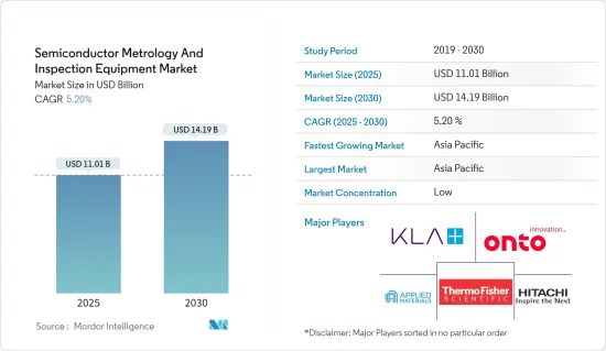
半導體測量和檢測設備市場規模預計在 2025 年為 110.1 億美元,預計到 2030 年將達到 141.9 億美元,預測期內(2025-2030 年)的複合年成長率為 5.2%。
主要亮點
- 半導體計量和檢測在控制半導體製造過程中發揮著至關重要的作用。半導體晶圓製造過程大約涉及400至600個步驟,可在一至兩個月內完成。如果在流程早期發現缺陷,則後續步驟的努力可能會白費。在半導體製造過程中,在關鍵時刻執行計量和檢查程序以確保特定的產量比率。
- 濱松光子學強調實現高產量比率以滿足當前半導體晶圓市場需求的重要性。計量和檢測在廣泛的半導體製造過程中發揮著至關重要的作用,以確保最佳的品質和產量比率。有效地表徵和測量薄膜、線寬、圖案缺陷和其他可能的缺陷對於快速解決任何問題並最大限度地減少昂貴的停機時間至關重要。在半導體檢測中,使用高強度紫外線光源對於縮短檢測時間並提高評估晶圓上圖案和薄膜的準確性至關重要。
- 半導體計量在半導體製造過程中發揮著至關重要的作用,它提供有關晶圓物理特性的詳細資訊,並有助於調整製造過程以滿足特定參數。這確保了可靠、高品質的半導體裝置的生產,同時最大限度地減少浪費,使製造過程保持經濟性和永續性。
- 半導體產業正在推動積體電路的發展,提高性能、速度和尺寸,從而帶來製造技術的進步。保持對程序的準確監控已成為製造業的重要要素。隨著台積電、英飛凌、高通和英特爾等公司加大對晶片生產的投資,預計後端對計量設備和服務的需求將會增加。
- 智慧型手機、消費性電子產品和汽車應用推動了對具有成本效益的半導體材料的需求。這些進步正在刺激無線技術(5G)和人工智慧等創新。此外,隨著物聯網設備的採用趨勢不斷擴大,半導體產業預計將投資物聯網設備以實現智慧產品。智慧型裝置的使用正在增加,隨著 5G 連接在全球範圍內的擴展,預計還會進一步增加。根據 GSMA 預測,到 2025 年,5G行動寬頻連線數將達到 11 億(11 億),同年 5G 部署預計將覆蓋全球人口的 34%。
- 為了在市場上站穩腳跟,供應商正在積極建立策略夥伴關係,以建立先進的多功能測試平台。最近,k-Space Associates 於 2023 年 1 月發布了其最新的薄膜計量工具 kSA XRF(X光螢光)。該工具專門設計用於精確測量無法透過光學方法可靠測量的薄膜厚度。它的有效性已在多種基板(包括玻璃板、晶片和基座)上的半導體和介電層的測量中得到證實。這些應用與太陽能、發電和其他薄膜技術領域尤其相關。
- 然而,預測期內的市場成長預計將受到高設置成本和缺乏處理測量系統的專業知識等因素的有效阻礙。為了克服這些挑戰,服務導向的參與者正在提供按需計量服務,並在精密尺寸計量領域提供專業擴展。
- 此外,該市場的成長也受到美國貿易爭端等宏觀經濟因素的挑戰。美國對中國實施了多項制裁,阻止其取得先進的半導體設備。由於中國在市場供應鏈中發揮關鍵作用,這些發展將對該市場的成長產生負面影響。
半導體測量和檢測設備市場趨勢
晶圓檢測大幅成長
- 隨著半導體裝置設計日益小型化,提高製造產量比率的挑戰變得更加突出。節點的縮小和複雜 3D 架構的引入為設計階段增加了更多步驟和複雜性。該過程涉及數百個步驟,任何階段的缺陷或電氣故障都可能影響整體生產效率。鑑於上市時間和產量比率對於新半導體設計成功的重要性,利用晶圓檢測工具對於確保每個階段的最佳性能至關重要。
- 預計未來幾年對晶圓檢測的需求將持續成長,原因是對3D積體電路的需求不斷成長。這些電路廣泛應用於記憶卡、智慧型手機、智慧卡和各種運算設備等小型半導體設備。 3D 電路在許多空間受限的應用中越來越受歡迎,例如攜帶式消費性電子產品、感測器、MEMS 和工業產品,因為它們透過速度、耐用性、更低的功耗和更輕的記憶體來提高整體產品性能。
- 經濟高效的雲端處理解決方案的日益普及,增加了對微處理器和數位訊號處理器等邏輯設備的需求。這主要是由於各行業對伺服器和資料中心系統的使用日益增加。此外,物聯網設備的普及也增加了微處理器的使用。這些設備擴大使用薄晶圓來改善溫度控制並最佳化性能。這些因素正在促進晶圓檢測市場的擴張。
- 300毫米晶圓在LED應用的廣泛採用也推動了全球薄晶圓檢測市場的成長。 300mm晶圓的產量比率較高,讓LED廠商享有規模經濟效益,增加盈利。隨著運作中的300毫米晶圓生產設施數量的不斷成長,預計300毫米晶圓的需求將大幅增加。
- 根據SEMI矽晶圓製造商集團(SMG)的年終分析,預計2023年全球矽晶圓出貨量將下降14.3%,達到126.02億平方英吋。同期晶圓營收也下滑10.9%至123億美元。不過,人們對未來仍抱持樂觀態度,預計 2024 年的復甦勢頭將持續到 2026 年。預計晶圓出貨量將創下新高,這得益於人工智慧 (AI)、高效能運算 (HPC)、5G、汽車和工業應用等多個領域對矽的需求不斷成長。
- 5G的引入以及對5G採用活動的投資增加預計將進一步推動晶片產業對晶圓和晶圓檢測工具的需求。根據愛立信2022年行動報告,預計未來五年北美將成為5G用戶普及率的全球領導者。預計到2027年該地區90%的用戶將是5G。報告進一步預測,到2027年西歐82%的用戶、波灣合作理事會80%的用戶和東北亞74%的用戶將是5G。在已經開始部署5G的印度,預計到2027年5G將佔到所有用戶數的40%左右。在全球範圍內,預計到2027年5G將占到所有用戶數的近一半,總合用戶數將達到44億人。
- 預計未來幾年 IT、物聯網、可再生能源、電動車、電訊和其他產業將大幅成長。此外,這些產業嚴重依賴無線技術。 IC和半導體的使用使得無線技術的應用成為可能。因此,晶圓檢測市場提供了許多機會。英飛凌、台積電、意法半導體、美光、英特爾、三星等半導體行業知名企業正在大力投資晶片生產活動,為不斷成長的市場需求做出了重大貢獻。
亞太地區佔市場主導地位
- 亞太地區是半導體產業生產和消費的主要地區之一。據SIA稱,亞太地區是最大的半導體市場,其中中國佔最大佔有率。電子產業的重大進步,加上對電視和智慧型手機等電子設備的日益依賴,預計將推動該地區對晶圓偵測的需求。此外,該地區的公司願意投入資金進行晶圓測試。
- 在半導體計量和測試設備市場,許多區域性公司已經形成了聯盟和夥伴關係。例如,中國晶片製造設備製造商深圳精拓自動化設備有限公司宣布,已與中國最大的晶片開發商華為海思半導體簽署了一份為期五年(2021-2025年)具有法律約束力的合作備忘錄。兩家公司旨在擴大半導體封裝工具開發的夥伴關係,打造一個自給自足、不受監管的產業。
- 地方政府為發展本地半導體產業所做的努力也為研究市場的成長創造了良好的前景。例如,中國國務院的《國家積體電路產業發展規劃》提出,到2030年,中國要在半導體產業的各個領域達到世界領先水準。此外,《中國製造2025》計畫也將先進半導體製造知識的成果作為中國未來經濟的重要要素。它高度重視在全國範圍內建立強大的製造業策略。
- 例如,2023年7月,中國第二大晶片代工廠華虹半導體揭露了融資212億元人民幣(29.5億美元)的計畫。這項策略措施符合中國實現半導體供應自給自足、克服美國技術封鎖的決心。與前期主要專注於晶片生產不同,國家積體電路基金二期大力投資國內半導體製造、設備及相關材料,以克服現有的障礙。
- 在美國關係持續緊張的背景下,韓國正計劃頒布自己的“晶片法案”,以支持其半導體產業。這些緊張局勢導致了對組裝和包裝等服務的需求,使得韓國對半導體產業的支持至關重要。 2023年3月,韓國國會通過了一項法案,旨在透過對企業提供稅收優惠和鼓勵投資來增強其主導的半導體產業。預計此類政府措施將為計量和測試等後端設備製造商創造更多機會,以擴大其在該地區的業務。
- 2023年3月,韓國電子巨頭三星宣布,計劃在未來20年內投資300兆韓元(相當於2308億美元),以支持韓國政府到2042年在龍仁市南山邑建立佔地710萬平方公尺的巨型半導體中心的舉措。這項策略性措施旨在加強韓國在競爭日益激烈的全球半導體市場中的地位,從而提振對晶圓測試、ATP等後端設備的需求。
- 此外,許多公司正致力於擴大業務範圍,以在不同領域獲取利潤。新北市政府宣布,荷蘭設備專家阿斯麥控股公司(ASML Holding NV)將於2024年在新北市林口區動工興建新廠。此外,日本電子半導體公司東京電子株式會社正在台南市南部科學園區設立事業據點,預計2024年底完工。這些投資預計將在測量檢測市場創造新的商機。
半導體測量和檢測設備產業概況
半導體測量和檢測設備市場由以下知名公司組成:應用材料公司、尼康計量公司和 KLA 公司。這些公司透過注重市場擴張和收購,不斷擴大業務規模。這些收購活動有效地推動了整個市場的成長。此外,領先的公司投入大量資源進行研發活動,以維持其市場地位並推動創新。整體而言,競爭依然激烈,這主要歸因於受調查市場中主要企業的強勁存在。
- 2023年12月,日立高新技術發表了暗場晶圓缺陷偵測設備的最新創新產品DI4600。這種最先進的工具專門用於檢查半導體生產線上的圖案化晶圓和缺陷。 DI4600配備專用伺服器,增強了資料處理能力,提高了顆粒和缺陷檢測能力。透過將此先進系統納入生產線,半導體製造商將能夠高精度地監控缺陷,從而隨著產量的增加提高產量比率和成本效率。
- 2023 年 7 月,應用材料公司宣布與弗勞恩霍夫光子微系統研究所 (IPMS) 開展開創性合作,在歐洲建立一流的半導體計量和製程分析技術中心。該創新中心旨在提供最先進的計量系統,以加速半導體研究並加強與歐洲各地晶片製造商和生態系統合作夥伴的研發活動,重點關注 ICAPS(物聯網、通訊、汽車、電力和感測器)市場領域。
其他福利:
- Excel 格式的市場預測 (ME) 表
- 3個月的分析師支持
目錄
第1章 引言
- 研究假設和市場定義
- 研究範圍
第2章調查方法
第3章執行摘要
第4章 市場洞察
- 市場概覽
- 產業吸引力-波特五力分析
- 供應商的議價能力
- 買家的議價能力
- 新進入者的威脅
- 替代品的威脅
- 競爭程度
- 評估主要宏觀趨勢的影響
第5章市場動態
- 市場促進因素
- 對高性能、低成本半導體的需求不斷增加
- 消費性電子產品對半導體晶圓的需求不斷增加
- 市場限制
- 設置成本高,且缺乏有效操作測量系統的專業知識
- 原料和製造成本高
第6章市場區隔
- 按類型
- 微影測量
- 覆蓋
- 尺寸測量裝置
- 掩模檢查和測量
- 晶圓檢測
- 薄膜計量
- 其他過程控制系統
- 微影測量
- 按地區
- 北美洲
- 歐洲
- 亞太地區
- 世界其他地區
第7章競爭格局
- 公司簡介
- KLA Corporation
- Applied Materials Inc.
- Onto Innovation Inc.
- Thermo Fisher Scientific Inc.
- Hitachi Hi-Technologies Corporation(Hitachi Limited)
- Nova Measuring Instruments Ltd
- ASML Holding NV
- Lasertec Corporation
- JEOL Ltd
- Nikon Metrology NV(Nikon Group)
- Camtek Limited
第8章投資分析
第9章:市場的未來
The Semiconductor Metrology And Inspection Equipment Market size is estimated at USD 11.01 billion in 2025, and is expected to reach USD 14.19 billion by 2030, at a CAGR of 5.2% during the forecast period (2025-2030).
Key Highlights
- Semiconductor metrology and inspection play a crucial role in the management of the semiconductor manufacturing process. The manufacturing process of semiconductor wafers involves approximately 400 to 600 steps, which can be completed within one to two months. Any shortcomings detected early on in the process can result in the wastage of all the efforts put into the subsequent steps. Metrology and inspection procedures are implemented at critical junctures of the semiconductor manufacturing process to guarantee a specific yield.
- Hamamatsu emphasizes the importance of achieving high production yields in order to satisfy the current market requirements for semiconductor wafers. Metrology and inspection play a vital role in the extensive semiconductor manufacturing process to guarantee optimal quality and yield. It is crucial to efficiently characterize and measure thin films, line widths, pattern flaws, and other possible defects to promptly address any issues and minimize expensive downtime. In semiconductor inspection, the utilization of higher radiance UV light sources is essential to reduce inspection durations and improve the precision of evaluating patterns and thin films on wafers.
- Semiconductor metrology plays a crucial role in the semiconductor manufacturing process by offering detailed information on the physical properties of the wafer and facilitating adjustments to the production process to meet specific parameters. This ensures the production of reliable semiconductor devices of high quality while minimizing wastage, thus maintaining the economic viability and sustainability of the manufacturing process.
- The semiconductor sector is continuously aiming for more compact integrated circuits that provide enhanced performance and speeds, resulting in progress in manufacturing techniques. Maintaining accurate oversight of procedures has emerged as a vital factor in manufacturing. With firms like TSMC, Infineon, Qualcomm, and Intel expanding their chip production investments, the demand for metrology equipment and services is expected to rise in the back-end process.
- The demand for cost-effective semiconductor materials is being fueled by smartphones, consumer electronics, and automotive applications. These advancements are inspiring innovations like wireless technologies (5G) and artificial intelligence. Additionally, the semiconductor industry is expected to invest in IoT devices to achieve smart products as the trend of adoption of IoT devices continues to grow. The utilization of smart devices is on the rise and is anticipated to increase further with the global expansion of 5G connections. As per the GSMA, it is estimated that 5G mobile broadband connections will reach 1,100 million (1.1 billion) by the year 2025, while the 5G deployment is expected to encompass 34% of the global population by the same year.
- In order to gain a strong foothold in the market, vendors are actively engaging in strategic partnerships to create advanced multifunction inspection platforms. Recently, k-Space Associates introduced its latest thin film metrology tool, the kSA XRF (X-ray fluorescence), in January 2023. This tool is specifically designed to accurately measure the thickness of films that cannot be reliably measured using optical methods. Its effectiveness has been demonstrated in measuring semiconductor and dielectric layers on various substrates such as glass panels, wafers, and susceptors. These applications are particularly relevant in the fields of solar energy, power generation, and other thin-film technologies.
- However, the market's growth during the forecast period is expected to be hindered efficiently by factors such as high setup costs and a lack of expertise in handling metrology systems. In order to overcome these challenges, service-oriented players are offering on-demand metrology services, providing a professional extension in the specialized field of precision dimensional metrology.
- Furthermore, the growth of the market studied is also challenged by macroeconomic factors, such as the US-China trade dispute. The United States has imposed several sanctions on China, preventing the country from accessing advanced semiconductor equipment. Since China plays a significant role in the market's supply chain, these trends negatively impact the growth of the market studied.
Semiconductor Metrology and Inspection Equipment Market Market Trends
Wafer Inspection to Witness Significant Growth
- As the design of semiconductor devices progresses toward smaller nodes, the challenge of increasing manufacturing yields becomes more pronounced. The introduction of smaller nodes and intricate 3D architectures leads to additional steps and heightened complexity in the design phase. With hundreds of steps in the process, any defect or electrical fault at any stage can impede overall production efficiency. Given the significance of time-to-market and time-to-yield in determining the success of a new semiconductor design, the utilization of wafer inspection tools is crucial to ensure optimal performance at each stage.
- The growing demand for wafer inspection is expected to be fueled by the increasing need for three-dimensional integrated circuits in the upcoming years. These circuits are widely used in small semiconductor devices such as memory cards, smartphones, smart cards, and various computing devices. Three-dimensional circuits are gaining popularity in numerous space-constrained applications like portable consumer electronics, sensors, MEMS, and industrial products, as they enhance overall product performance in terms of speed, durability, low power consumption, and lightweight memory.
- The increasing availability of cost-effective cloud computing solutions has led to a rise in demand for logic devices such as microprocessors and digital signal processors. This is primarily driven by the growing use of server and data center systems in various industries. Furthermore, the proliferation of IoT-enabled devices has resulted in a higher usage of microprocessors. Thin wafers are increasingly utilized in these devices to enhance temperature control and optimize performance. These factors collectively contribute to the expansion of the wafer inspection market.
- The widespread adoption of 300 mm wafers in LED applications is also a key driver for the global growth of the thin wafer inspection market. These wafers offer higher yields, enabling LED manufacturers to achieve economies of scale and enhance profitability. As the number of operational 300 mm wafer production facilities continues to increase, the demand for 300 mm wafers is expected to witness a significant surge.
- According to the year-end analysis conducted by the SEMI Silicon Manufacturers Group (SMG), global silicon wafer shipments experienced a decline of 14.3% in 2023, reaching 12,602 million square inches. Additionally, wafer revenue contracted by 10.9% to USD 12.3 billion during the same period. However, there is optimism for the future as the momentum from the 2024 rebound is expected to continue until 2026. This positive trend is anticipated to result in new record-high wafer shipments, driven by the increasing demand for silicon in various sectors such as artificial intelligence (AI), high-performance computing (HPC), 5G, automotive, and industrial applications.
- The introduction of 5G and increasing investments in the 5G adoption activities are further expected to drive the demand for wafers and wafer inspection tools in the chip industry. According to the Ericsson Mobility Report 2022, North America is projected to be the global leader in 5G subscription penetration over the next five years. It is anticipated that 90% of subscriptions in the region will be 5G by 2027. Additionally, the report predicts that by 2027, 82% of subscriptions in Western Europe, 80% in the Gulf Cooperation Council, and 74% in North-East Asia will be 5G. In India, where 5G deployments have already begun, it is expected that 5G will account for approximately 40% of all subscriptions by 2027. Globally, 5G is expected to represent nearly half of all subscriptions by 2027, reaching a total of 4.4 billion subscriptions.
- The IT, IoT, renewable, EVs, telecom, and other sectors are poised for substantial growth in the upcoming years. Additionally, these sectors heavily rely on wireless technology. The utilization of ICs and semiconductors enables the application of wireless technology. As a result, the wafer inspection market is presented with a multitude of opportunities. Prominent companies in the semiconductor industry, such as Infineon, TSMC, ST, Micron, Intel, Samsung, and others, are making significant investments in chip production activities, which can greatly contribute to the market's increased demand.
Asia-Pacific to Dominate the Market
- Asia-Pacific is one of the prominent regions in the semiconductor industry in terms of manufacturing and consumption. According to SIA, Asia-Pacific is the largest regional semiconductor market, and China accounts for the most significant share in the region. The significant advancements in the electronics sector, combined with the growing reliance on electronic gadgets like televisions and smartphones, are anticipated to boost the requirement for wafer inspection in the region. Furthermore, companies situated in this area are prepared to allocate funds toward the utilization of wafer inspections.
- Many regional companies are entering collaborations and partnerships in the semiconductor metrology/inspection equipment market. For instance, Shenzhen JT Automation Equipment, a chip production tool manufacturer in China, announced a legally binding five-year (2021-2025) memorandum of understanding with Huawei's HiSilicon Technologies, China's largest chip developer. Both firms aim to extend their partnership for the development of semiconductor packaging tools, creating a self-sufficient and regulated industry.
- The regional government's initiatives to develop the local semiconductor industry also create a favorable outlook for the growth of the market studied. For instance, China's State Council's "National Integrated Circuit Industry Development Guidelines" aim to make the country a global leader in all segments of the semiconductor industry by 2030. Additionally, the Made in China 2025 initiative maintains achieving knowledge concerning advanced semiconductor manufacturing as a vital component of China's future economy. It is highly focused on building a strategy for strong manufacturing nationwide.
- For instance, in July 2023, Hua Hong Semiconductor, the second-largest chip foundry in China, revealed its plan to raise CNY 21.2 billion (USD 2.95 billion). This strategic move is in line with China's determined efforts to attain self-sufficiency in semiconductor supply and overcome the technology blockade imposed by the United States. In contrast to the initial phase that primarily concentrated on chip production, the China IC Fund II has made significant investments in domestic semiconductor manufacturing, equipment, and associated materials to overcome the existing obstacles.
- South Korea plans to enact its own version of the "Chips Act" in order to bolster its semiconductor industry amid the ongoing tensions between the United States and China. These tensions have created a demand for services such as assembly and packaging, making it crucial for South Korea to support its semiconductor industry. In March 2023, the country's parliament passed legislation to strengthen its dominant semiconductor industry by providing tax benefits to businesses and encouraging investments. Such government initiatives are expected to boost the opportunities for the backend equipment markers, such as metrology and inspection, to enhance their presence in the region.
- In March 2023, Samsung, the Korean electronics giant, announced its intention to invest KRW 300 trillion (equivalent to USD 230.8 billion) over the next two decades in support of the South Korean government's initiative to establish a massive semiconductor hub spanning 7.1 million square meters in Namsayup, Yongin, by 2042. This strategic move is designed to bolster Korea's position in the increasingly competitive global semiconductor market, consequently driving up the demand for backend equipment such as wafer testing, ATP, and other equipment.
- Additionally, numerous enterprises are focusing on expanding their activities to boost profits in different sectors. The New Taipei City government announced that ASML Holding NV, a Dutch company that specializes in semiconductor equipment, will commence the construction of its new facility in the Linkou District of New Taipei City in the fiscal year 2024. Moreover, Tokyo Electron Ltd, a Japanese electronics and semiconductor corporation, is making progress in establishing its operations hub in the Southern Taiwan Science Park in Tainan, with plans to complete it by the end of 2024. These investments have the potential to create opportunities in the metrology and inspection market.
Semiconductor Metrology and Inspection Equipment Industry Overview
The semiconductor metrology and inspection equipment market comprises prominent players such as Applied Materials Inc., Nikon Metrology NV, and KLA Corporation. These firms have continuously expanded their operation scales by focusing on market expansions and acquisitions. Acquisition activities effectively set the ball rolling regarding the overall growth of the market studied. Large companies have also been expending significant resources on R&D operations to protect their market position and drive innovation in the market studied. Overall, the degree of competition remains high, primarily driven by the strong presence of prominent players involved in the market studied.
- In December 2023, Hitachi High-Tech Corporation unveiled the DI4600, the latest innovation in its Dark Field Wafer Defect Inspection System. This state-of-the-art tool is specifically designed to inspect particles and defects on patterned wafers in semiconductor production lines. With its dedicated server, the DI4600 offers enhanced data processing power, enabling improved detection capabilities for particles and defects. By incorporating this advanced system into their production lines, semiconductor manufacturers can ensure highly accurate defect monitoring, resulting in increased yields and cost efficiency as production volumes continue to rise.
- In July 2023, Applied Materials Inc. and the Fraunhofer Institute for Photonic Microsystems IPMS announced a pioneering collaboration to create the premier technology center for semiconductor metrology and process analysis in Europe. This innovative hub is designed to provide state-of-the-art metrology systems to accelerate semiconductor research and enhance development efforts with chipmakers and ecosystem partners across Europe, with a specific focus on ICAPS (Internet of Things, communications, automotive, power, and sensors) market segments.
Additional Benefits:
- The market estimate (ME) sheet in Excel format
- 3 months of analyst support
TABLE OF CONTENTS
1 INTRODUCTION
- 1.1 Study Assumptions and Market Definition
- 1.2 Scope of the Study
2 RESEARCH METHODOLOGY
3 EXECUTIVE SUMMARY
4 MARKET INSIGHTS
- 4.1 Market Overview
- 4.2 Industry Attractiveness - Porter's Five Forces Analysis
- 4.2.1 Bargaining Power of Suppliers
- 4.2.2 Bargaining Power of Buyers
- 4.2.3 Threat of New Entrants
- 4.2.4 Threat of Substitutes
- 4.2.5 Degree of Competition
- 4.3 An Assessment of the Impact of Key Macro Trends
5 MARKET DYNAMICS
- 5.1 Market Drivers
- 5.1.1 Increasing Demand for High-performance, Low-cost Semiconductors
- 5.1.2 Increasing Demand for Semiconductor Wafers in Consumer Electronics
- 5.2 Market Restraints
- 5.2.1 High Setup Cost and Lack of Expertise in Handling Metrology Systems Efficiently
- 5.2.2 High Raw Material and Fabrication Costs
6 MARKET SEGMENTATION
- 6.1 By Type
- 6.1.1 Lithography Metrology
- 6.1.1.1 Overlay
- 6.1.1.2 Dimension Equipment
- 6.1.1.3 Mask Inspection and Metrology
- 6.1.2 Wafer Inspection
- 6.1.3 Thin Film Metrology
- 6.1.4 Other Process Control Systems
- 6.1.1 Lithography Metrology
- 6.2 By Geography
- 6.2.1 North America
- 6.2.2 Europe
- 6.2.3 Asia-Pacific
- 6.2.4 Rest of the World
7 COMPETITIVE LANDSCAPE
- 7.1 Company Profiles
- 7.1.1 KLA Corporation
- 7.1.2 Applied Materials Inc.
- 7.1.3 Onto Innovation Inc.
- 7.1.4 Thermo Fisher Scientific Inc.
- 7.1.5 Hitachi Hi-Technologies Corporation (Hitachi Limited)
- 7.1.6 Nova Measuring Instruments Ltd
- 7.1.7 ASML Holding NV
- 7.1.8 Lasertec Corporation
- 7.1.9 JEOL Ltd
- 7.1.10 Nikon Metrology NV (Nikon Group)
- 7.1.11 Camtek Limited
8 INVESTMENT ANALYSIS
9 FUTURE OF THE MARKET
 半導體計量與測試市場分析及預測(至2035年):依類型、產品類型、服務、技術、組件、應用、裝置、製程及最終用戶分類
 半導體測量和測試設備市場:按測試類型、技術、晶圓廠類型、製程節點、國家和地區分類-全球產業分析、市場規模、市場佔有率和預測(2025-2032 年)
 半導體計量和檢測設備市場規模、佔有率、成長及全球產業分析:依類型、應用和地區劃分的洞察與預測(2026-2034)
 2026年全球半導體計量與測試市場報告
 按技術、光罩類型、晶圓尺寸、應用和最終用途行業分類的光罩檢測和計量設備市場 - 全球預測 2026-2032半導體計量和檢測設備市場-2025-2030年預測
 模具分類設備:全球市佔率及排名、總收入及需求預測(2025-2031年)光罩檢測和計量設備 - 全球市場佔有率和排名、總收入和需求預測(2025-2031 年)
 半導體計量和檢測設備市場預測至2032年:按設備類型、技術、應用、最終用戶和地區分類的全球分析
 半導體計量和檢測設備市場規模、佔有率和趨勢分析報告:按技術、尺寸、製程節點、晶圓廠類型、地區和細分市場預測,2025 年至 2033 年