


 |
市場調查報告書
商品編碼
1685832
先進封裝:市場佔有率分析、產業趨勢與統計、成長預測(2025-2030)Advanced Packaging - Market Share Analysis, Industry Trends & Statistics, Growth Forecasts (2025 - 2030) |
||||||
※ 本網頁內容可能與最新版本有所差異。詳細情況請與我們聯繫。
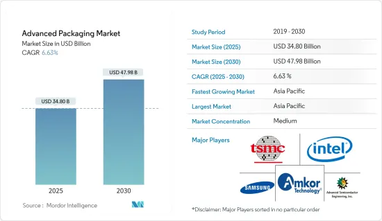
先進封裝市場規模預計在 2025 年為 348 億美元,預計到 2030 年將達到 479.8 億美元,預測期內(2025-2030 年)的複合年成長率為 6.63%。
主要亮點
- 先進封裝是指在傳統積體電路封裝之前對元件進行整合和互連。它允許整合多個設備,包括電氣、機械和半導體元件,並將它們封裝到單一電子設備中。與傳統的積體電路封裝不同,先進封裝採用在半導體製造設備中執行的製程和技術。它介於製造和傳統封裝之間,包括 3D IC、2.5D IC、扇出型晶圓級封裝和系統級封裝等多種技術。
- 先進封裝可以透過在一個封裝內整合多個晶片來實現更高的性能。透過使用穿透矽通孔、內插器、橋接器和簡單電線等技術連接這些晶片,我們可以提高訊號速度並減少驅動這些訊號所需的能量。此外,先進的封裝允許混合在不同製程節點上開發的組件。
- 3D整合、異質整合等先進封裝技術可顯著提高積體電路和記憶體晶片的效能。這些技術可以提高功能密度、互連密度以及針對特定應用的記憶體客製化。例如,記憶體整合設備製造商(IDM)可以使用3D堆疊技術來提高記憶體晶片的效能,並為特定客戶客製化記憶體。
- 此外,先進的封裝技術可以使電子元件小型化,而不會影響效能。在先進封裝中,類比工具和多物理方法來評估和確保設計的熱可靠性和訊號完整性。在設計階段早期識別潛在的封裝問題,可以讓積體電路設計人員在原型設計之前進行修正,以提高可靠性。
- 在全球金融危機之後,法規結構的變化和後危機市場環境對先進封裝市場產生了重大影響。為了保持市場競爭力,OSAT 正在活性化其併購活動。預計這一趨勢將在未來幾年持續下去,主要企業之間將出現不同程度的整合。
- 由於晶片製造商已經在努力應對日益成長的複雜性、莫耳定律變得更加困難和昂貴而導致的未來設計藍圖的丟失,以及標準不斷發展和規則集不同的新市場的湧入,整合可能會繼續下去。收購可能會對我們現有技術的產品支援和服務產生重大影響。對於預計設備使用壽命為 10 至 20 年左右的市場來說,這尤其令人不安。預計這將抑制市場成長。
先進封裝市場趨勢
嵌入式晶粒呈現強勁成長率
- 全球嵌入式晶粒封裝技術的成長主要受到5G網路技術和家用電子電器需求不斷成長的推動。許多家用電子電器,如智慧型手機、筆記型電腦、平板電腦和掌上遊戲機,都包含多個嵌入式晶片,以提供更好的使用者介面和增強的整體效能。在智慧型手機、穿戴式裝置和其他家用電子電器中,這些晶片主要用於DC-DC轉換器、電力電子電路和攝影機電路。
- 此外,由於其架構內建了 5G,汽車智慧視訊監控系統中使用的嵌入式設備的響應時間變得更快。此外,微電子設備中的電路也迫切需要小型化。嵌入式晶粒封裝因其在高頻下的優異電氣性能而成為新興微波應用的一種很有前途的技術。隨著電子設備體積越來越小以便於使用,對緊湊型電子電路的需求也日益增加。嵌入式晶粒封裝技術滿足了這一需求,該技術具有許多優勢,例如增強了電子電路的功能和效率,減小了尺寸、降低了訊號電感和功率電感,提高了可靠性,並增加了訊號密度。
- 5G網路的日益普及將推動市場發展。例如,愛立信預計,2019年至2028年期間,全球5G用戶數將大幅成長,從1,200萬多成長至45億多萬。按地區分類,東南亞、東北亞、尼泊爾、印度和不丹預計訂閱量將出現最大增幅。
- 此外,5G 技術的推出需要緊湊高效的設備來支援複雜的通訊系統。晶圓級晶片規模封裝 (WLCSP) 和扇出型封裝等先進封裝解決方案可實現更小的外形規格、低耗電量和更好的溫度控管,使其適用於 5G 設備。
- 此外,嵌入式晶粒解決方案的 3D 封裝作為下一代設備的整合工具正在引起消費者的關注,並可能成為未來幾年的主要趨勢。因此,預計它將在預測期內推動市場發展。
預計亞太地區將出現顯著成長
- 由於主要半導體製造商的存在、快速的工業化以及龐大的消費性電子市場,亞太地區有望成為半導體封裝市場的主導者。該地區以半導體的大量生產和在消費性電子、汽車和通訊等不同行業採用先進的封裝技術而聞名。預計這些因素將推動亞太半導體封裝市場的成長,並為市場相關人員提供有利可圖的機會。
- 中國制定了非常雄心勃勃的半導體計劃,並獲得了 1500 億美元的巨額預算支持。該國正在發展國內積體電路產業,以提高晶片產量。大中華區由中國香港和台灣組成,是重要的地緣政治熱點。美國之間正在進行的貿易戰進一步加劇了該地區的緊張局勢,該地區是所有主要工藝技術的發源地,促使多家中國公司投資半導體產業。
- 例如,2023 年 9 月,中國宣布計劃推出一項新的國家支持的投資基金,為半導體產業籌集約 400 億美元。 2022年12月,中國宣布將投入超過1兆元(1,430億美元)支持其半導體產業。該舉措是朝著實現晶片生產自給自足邁出的重要一步,也是對美國阻礙中國技術進步的行動的回應。預計預測期內包裝服務的需求將大幅成長。
- 在私營部門投資方面,中國在許多此類聲明中一直處於領先地位,特別是在封裝技術的發展方面,使其成為所有尋求擴大半導體產業的經濟體的主要競爭對手。例如,2023年8月,中國國家自然科學基金委員會(NSFC)宣布將向30個Chiplet計劃投資640萬美元。
- 此外,2023年8月,台灣半導體製造公司(TSMC)宣布,將投資900億新台幣在台灣建造一座先進的晶片封裝工廠,以滿足全球不斷成長的需求。此外,儘管中國政府認為美光公司的產品存在安全風險,美光公司仍於2023年6月承諾投資數百萬美元在中國建廠。美光公司表示,未來幾年將投資總計 43 億元人民幣(略高於 6 億美元)升級其西安晶片封裝工廠。
先進封裝市場概覽
先進封裝市場處於半固體狀態,主要企業包括日月光半導體製造股份有限公司、台灣半導體製造股份有限公司、安靠科技、英特爾公司和 JCIVE 集團。
- 2023 年 7 月,安靠科技展示了在使用台積電先進的低 k 製程技術製造的設備進行引線鍵合和覆晶構裝的開發和檢驗方面的廣泛舉措和成就。 Amkor 已與多家客戶合作以驗證其低 k 產品,並計劃在今年稍後大幅增加其低 k 封裝的產量。
- 2022年11月,英特爾公司在檳城破土動工建造新的半導體組裝和測試工廠。該工廠由兩棟建築(4號工廠和5號工廠)組成,位於峇六拜自由工業區內,總面積為 982,000 平方英尺,預計於 2025 年竣工,預計將為當地市場創造 2,700 個就業機會。
其他福利
- Excel 格式的市場預測 (ME) 表
- 3個月的分析師支持
目錄
第1章 引言
- 研究假設和市場定義
- 研究範圍
第2章調查方法
第3章執行摘要
第4章 市場洞察
- 市場概覽
- 產業價值鏈分析
- 產業吸引力-波特五力分析
- 新進入者的威脅
- 買家的議價能力
- 供應商的議價能力
- 替代品的威脅
- 競爭對手之間的競爭強度
- 評估新冠疫情和宏觀經濟趨勢對產業的影響
第5章市場動態
- 市場促進因素
- 電子產品向先進架構發展的趨勢
- 新興國家有利的政府法規和政策
- 市場限制
- 市場整合影響整體盈利
第6章市場區隔
- 按包裝平台
- 覆晶
- 嵌入式晶粒
- Fi-WLP
- Fo-WLP
- 2.5D/3D
- 按地區
- 北美洲
- 歐洲
- 亞洲
- 澳洲和紐西蘭
- 拉丁美洲
- 中東和非洲
第7章競爭格局
- 公司簡介
- Amkor Technology Inc.
- Taiwan Semiconductor Manufacturing Company Limited
- Advanced Semiconductor Engineering Inc.
- Intel Corporation
- JCET Group Co. Ltd
- Chipbond Technology Corporation
- Samsung Electronics Co. Ltd
- Universal Instruments Corporation
- ChipMOS Technologies Inc.
- Brewer Science Inc.
第8章投資分析
第9章 市場機會與未來趨勢
The Advanced Packaging Market size is estimated at USD 34.80 billion in 2025, and is expected to reach USD 47.98 billion by 2030, at a CAGR of 6.63% during the forecast period (2025-2030).
Key Highlights
- Advanced packaging refers to the aggregation and interconnection of components before traditional integrated circuit packaging. It allows multiple devices, such as electrical, mechanical, or semiconductor components, to be merged and packaged as a single electronic device. Unlike traditional integrated circuit packaging, advanced packaging employs processes and techniques that are performed at semiconductor fabrication facilities. It sits in between fabrication and traditional packaging, and it includes various technologies like 3D ICs, 2.5D ICs, fan-out wafer-level packaging, system-in-package, etc.
- Advanced packaging can achieve performance gains through the integration of multiple chips in a package. By connecting these chips using fatter, such as through-silicon vias, interposers, bridges, or simple wires, the speed of signals can be increased, and the amount of energy required to drive those signals can be reduced. Additionally, advanced packaging allows for the mixing of components developed at different process nodes.
- Advanced packaging techniques, such as 3D integration and heterogenous integration, can significantly improve the performance of integrated circuits and memory chips. These techniques allow for increased feature density, interconnect density, and customization of memory for specific applications. For instance, memory-integrated device manufacturers (IDMs) can use 3D stacking technology to enhance performance in memory chips and customize memory for specific clients.
- Advanced packaging techniques also enable the reduction of the size of electronic components without compromising their performance. Simulation tools and Multiphysics approaches are used in advanced packaging to assess and ensure the thermal reliability and signal integrity of designs. By identifying potential packaging problems early in the design phase, integrated circuit designers can make modifications to improve reliability before prototyping.
- The experience of the global financial crisis changes to regulatory frameworks and the post-crisis market environment has had a significant impact on the advanced packaging market. To remain competitive in the market, OSATs are increasing their M&A activities. This will continue throughout the coming years, with various levels of consolidation among the major players.
- The consolidation will increase as chipmakers are already grappling with the increasing complexity, the loss of a roadmap for future designs as Moore's Law is becoming more difficult and expensive to sustain, and a flood of new markets with evolving standards and different sets of rules. Acquisitions can have a big impact on product support and servicing of the existing technology. This is particularly troublesome for markets in which the devices are expected to function for about 10 to 20 years. This is expected to restrain the growth of the market..
Advanced Packaging Market Trends
Embedded Die to Witness Significant Growth Rate
- The growth of global embedded die packaging technology is majorly driven by the increasing demand for 5G network technology and consumer electronics. Numerous consumer electronic devices, such as smartphones, laptops, tablets, and portable gaming consoles, incorporate several embedded chips to provide a better user interface and enhanced overall performance. In smartphones, wearable devices, and other consumer electronic appliances, these chips are used primarily in DC-DC converters, power electronic circuitry, and camera circuits.
- Moreover, due to the incorporation of 5G into their architecture, embedded devices used in smart video surveillance systems of automobiles give rapid response times. There is also a critical need for circuit miniaturization in microelectronic devices. Embedded die packaging is a promising technology for emerging microwave applications, owing to its excellent electrical performance at high frequencies. With the reduction in size of electronic devices for ease of access for users, the demand for compact electronic circuitry is on the rise. This demand is met by embedded die packaging technology, which offers advantages such as increased functionality and efficiency of the electronic circuit; reduced size, signal inductance, and power inductance; improved reliability; and higher signal density.
- The increasing adoption of 5G networks would augment the development of the studied market. For instance, according to Ericsson, 5G subscriptions are forecasted to increase drastically worldwide from 2019 to 2028, from over 12 million to over 4.5 billion subscriptions, respectively. Southeast Asia, Northeast Asia, Nepal, India, and Bhutan are expected to have the most subscriptions by region.
- Also, the rollout of 5G technology requires compact and efficient devices to accommodate complex communication systems. Advanced packaging solutions like Wafer Level Chip Scale Package (WLCSP) and fan-out packaging enable smaller form factors, lower power consumption, and enhanced thermal management, making them suitable for 5G devices.
- Furthermore, 3D packaging with embedded die solutions is gaining attention among consumers as an integration tool for next-generation devices, which is likely to become a key trend in the future. Hence, it is anticipated to drive the market over the forecast period.
Asia Pacific is Expected to Witness Significant Growth Rate
- The Asia Pacific region is anticipated to emerge as a dominant player in the semiconductor packaging market, owing to the presence of major semiconductor manufacturers, rapid industrialization, and a vast consumer electronics market. The region is renowned for its high-volume production of semiconductors and the adoption of advanced packaging technologies across diverse industries, such as consumer electronics, automotive, and telecommunications. These factors are expected to fuel the growth of the semiconductor packaging market in the Asia Pacific region, thereby presenting lucrative opportunities for market players.
- China has a highly ambitious semiconductor agenda, supported by a substantial funding of USD 150 billion. The nation is developing its domestic IC industry to increase its chip production. The Greater China region, comprising Hong Kong, China, and Taiwan, is a significant geopolitical hotspot. The ongoing US-China trade war has further intensified tensions in this area, which houses all the leading process technology, prompting several Chinese firms to invest in their semiconductor industry.
- For instance, in September 2023, China announced its plans to launch a new state-backed investment fund to raise about USD 40 billion for its semiconductor sector. In December 2022, China announced its commitment to a support package exceeding YUAN 1 trillion (USD 143 billion) for its semiconductor industry. This initiative is a crucial step towards achieving self-sufficiency in chip production and is a response to U.S. actions aimed at hindering China's technological progress. The demand for packaging services is anticipated to rise considerably over the forecasted period, owing to the region's intensified efforts to enhance domestic chip manufacturing.
- Regarding investments from private players, the country has been at the forefront for many such announcements, especially toward evolving packaging technologies, thus presenting it as a major competitor for all national geographies working towards expanding its semiconductor industry. For instance, in August 2023, the National Natural Science Foundation of China (NSFC) announced an investment of USD 6.4 million in 30 Chiplet projects, now considered the next big advanced packaging technology.
- Moreover, in August 2023, Taiwan Semiconductor Manufacturing Company (TSMC) announced investing 90 billion New Taiwan dollars to build an advanced chip packaging plant in Taiwan amid booming global demand. Additionally, Micron stated in June 2023 that it would spend millions of dollars on a factory in China despite the Chinese government having just deemed its goods a security risk. Over the coming years, Micron stated it will upgrade its chip packaging factory in Xi'an with investments totaling YUAN 4.3 billion (slightly over USD 600 million).
Advanced Packaging Market Overview
The Advanced Packaging Market had a semi-consolidated landscape with key players like Advanced Semiconductor Engineering Inc., Taiwan Semiconductor Manufacturing Company Limited, Amkor Technology, Intel Corporation, and JCET Group Co. Ltd. A significant shift was noted as numerous IC manufacturers transitioned to sub-advanced packaging, spurring market demand and heightening competition.
- In July 2023 - Amkor Technology extensively detailed its efforts and achievements in developing and validating wire bond and flip chip packaging for devices manufactured using TSMC's advanced low-k process technologies. Collaborating with multiple clients on low-k product qualification, Amkor aimed for a substantial volume ramp-up in low-k packages during the latter half of the year.
- In November 2022 - Intel Corporation commenced work on a new semiconductor assembly and testing facility in Penang. Comprising two buildings (Plants 4 and 5) totaling 982,000 square feet within the Bayan Lepas Free Industrial Zone, this facility, expected to be finalized by 2025, was anticipated to generate 2,700 job opportunities within the local market.
Additional Benefits:
- The market estimate (ME) sheet in Excel format
- 3 months of analyst support
TABLE OF CONTENTS
1 INTRODUCTION
- 1.1 Study Assumptions and Market Definition
- 1.2 Scope of the Study
2 RESEARCH METHODOLOGY
3 EXECUTIVE SUMMARY
4 MARKET INSIGHTS
- 4.1 Market Overview
- 4.2 Industry Value Chain Analysis
- 4.3 Industry Attractiveness - Porter's Five Forces Analysis
- 4.3.1 Threat of New Entrants
- 4.3.2 Bargaining Power of Buyers
- 4.3.3 Bargaining Power of Suppliers
- 4.3.4 Threat of Substitute Products
- 4.3.5 Intensity of Competitive Rivalry
- 4.4 Assessment of the Impact of COVID-19 and Macro Economic Trends on the Industry
5 MARKET DYNAMICS
- 5.1 Market Drivers
- 5.1.1 Increasing Trend of Advanced Architecture in Electronic Products
- 5.1.2 Favorable Government Policies and Regulations in Developing Countries
- 5.2 Market Restraints
- 5.2.1 Market Consolidation affecting Overall Profitability
6 MARKET SEGMENTATION
- 6.1 By Packaging Platform
- 6.1.1 Flip Chip
- 6.1.2 Embedded Die
- 6.1.3 Fi-WLP
- 6.1.4 Fo-WLP
- 6.1.5 2.5D/3D
- 6.2 By Geography
- 6.2.1 North America
- 6.2.2 Europe
- 6.2.3 Asia
- 6.2.4 Australia and New Zealand
- 6.2.5 Latin America
- 6.2.6 Middle East and Africa
7 COMPETITIVE LANDSCAPE
- 7.1 Company Profiles
- 7.1.1 Amkor Technology Inc.
- 7.1.2 Taiwan Semiconductor Manufacturing Company Limited
- 7.1.3 Advanced Semiconductor Engineering Inc.
- 7.1.4 Intel Corporation
- 7.1.5 JCET Group Co. Ltd
- 7.1.6 Chipbond Technology Corporation
- 7.1.7 Samsung Electronics Co. Ltd
- 7.1.8 Universal Instruments Corporation
- 7.1.9 ChipMOS Technologies Inc.
- 7.1.10 Brewer Science Inc.
8 INVESTMENT ANALYSIS
9 MARKET OPPORTUNITIES AND FUTURE TRENDS
 先進封裝技術市場預測(至2032年):按封裝技術、互連方法、材料類型、裝置架構、最終用戶和地區進行的全球分析
 2025年全球先進封裝技術市場報告
 GMIPulse - 包裝市場情報訂閱
 美國飲料包裝設備市場:市場規模、佔有率、趨勢分析(按類型、自動化程度和應用)、細分市場預測(2025-2033)下一代封裝市場:按封裝類型、應用和地區分類自冷包裝市場機會、成長動力、產業趨勢分析及 2025 - 2034 年預測石墨烯注入包裝市場機會、成長動力、產業趨勢分析及 2025 - 2034 年預測先進封裝市場規模、佔有率、趨勢分析報告:按封裝類型、應用、地區、細分市場預測,2025-2030
 2025 年至 2033 年先進封裝市場規模、佔有率、趨勢及預測(按類型、最終用途和地區)先進封裝市場機會、成長動力、產業趨勢分析及 2025-2034 年預測