


 |
市場調查報告書
商品編碼
1630220
記憶體封裝:市場佔有率分析、產業趨勢與統計、成長預測(2025-2030)Memory Packaging - Market Share Analysis, Industry Trends & Statistics, Growth Forecasts (2025 - 2030) |
||||||
※ 本網頁內容可能與最新版本有所差異。詳細情況請與我們聯繫。
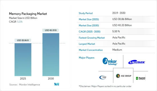
記憶體封裝市場規模預計到 2025 年為 308.6 億美元,預計到 2030 年將達到 403.3 億美元,預測期內(2025-2030 年)複合年成長率為 5.5%。
最近的COVID-19疫情預計將導致受訪市場供應鏈出現嚴重失衡,其中亞太地區,尤其是中國,是受訪市場的主要影響因素之一。此外,亞太地區許多地方政府正在對半導體產業進行長期投資,因此預計將恢復市場成長。例如,中國政府已為國家積體電路投資基金2030年第二期籌集約230億至300億美元。全球多個地區的經濟影響對半導體市場的成長構成重大挑戰,因為市場從疫情中恢復的時間尚不確定,而先進記憶體封裝市場所需的關鍵原料的供應預計將直接影響半導體市場的成長。全球性別的影響。
主要亮點
- 記憶體採用多種封裝技術,包括覆晶、導線架、引線鍵合和矽通孔 (TSV)。隨著晶片變得更小、更複雜,與外部電路的電氣連接數量也隨之增加。
- 這也帶動了封裝技術的發展。覆晶、TSV 和晶圓級晶片級封裝 (WLCSP) 是很有前途的技術,可滿足寬頻化、高速和更小/更薄封裝的需求。易於理解的程式調整、低工程成本和輕鬆轉換正在推動對打線接合記憶體封裝平台的需求。
- 此外,隨著封裝設計的變化,引線鍵合記憶體平台由於其靈活性、可靠性和低成本而繼續被用作最優選的互連平台。覆晶於 2016 年開始進入 DRAM 記憶體封裝領域,並且由於高頻寬需求推動 DRAM PC/伺服器的採用增加,預計覆晶將會成長。
- 記憶體晶片的高頻寬和低延遲正在推動許多應用中對高效能運算的需求,高頻寬記憶體正在採用矽穿孔電極(TSV)。
記憶體封裝市場趨勢
DRAM預計將佔據較大佔有率
- 市場正在見證移動和計算(主要是伺服器)的需求。每支智慧型手機的 DRAM 記憶體容量預計將平均增加三倍以上,到 2022 年達到約 6GB。
- 最近,研究市場的主導廠商之一三星電子宣布批量生產用於高階智慧型手機的新型記憶體封裝。
- 對於行動應用,引線鍵合平台預計將主導記憶體封裝。然而,高階智慧型手機向多晶片封裝(ePoP)的過渡可能很快就會開始。隨著企業架構和雲端運算的改進,運算 DRAM 封裝預計將在預測期內顯著成長。
- 三星的 HBM2 技術由 8 個 8Gbit DRAM晶粒組成,使用 5,000 個 TSV 堆疊在一起。最近,該公司還發布了新的 HBM 版本,可堆疊 12 個 DRAM晶粒,並使用 60,000 個 TSV 將它們連接起來。
- 每部智慧型手機的 DRAM 記憶體容量正在增加,新裝置至少提供 4GB 容量,預計到 2020 年將達到至少 6GB 至 8GB 容量。每部智慧型手機的 NAND 容量正在不斷增加,目前已超過 64GB,預計到 2020 年將達到 150GB 以上。對於伺服器而言,到 2020 年,每台伺服器的 DRAM 容量預計將增加到約 1TB,而企業級 SSD NAND 容量預計到預測期結束時將達到 5TB 以上。
汽車工業佔有很大佔有率
- 在自動駕駛和車載資訊娛樂趨勢的推動下,使用低密度(低 MB)記憶體的汽車市場可能會增加 DRAM 記憶體的採用。由於觸控顯示器驅動IC、AMOLED顯示器和工業IoT等新領域的應用,NOR快閃記憶體封裝市場預計也將成長。
- 作為其成長策略的一部分,許多 OSAT 廠商已與記憶體晶片製造商建立策略聯盟,而區域廠商正在與全球技術供應商合作,以擴大其市場影響力。
- 市場上的製造商正在擴大其生產設施。例如,SK海力士公司正在擴大其在韓國的半導體封裝和測試設施的產能。這些發展可能會增加現有參與者的市場開發機會,並為競爭對手提供市場優勢。
- 封裝技術中引入的創新與大型系統晶片(SoC) 解決方案中功能密度的增加有關。然而,汽車環境中嚴格的可靠性要求和 OSAT 行業不斷變化的模式預計將阻礙預測期內的市場成長。
- 最近,矽基感測器技術在生物辨識感測器、CMOS 影像感測器和加速計等 MEMS 感測器等各種應用中的使用有所增加。此外,整合到行動裝置(例如行動電話和 PDA)中的感測器裝置的數量正在增加。對於這些應用,小尺寸、低成本且易於整合對於成功整合此感測器技術至關重要。
- 一般來說, OEM更喜歡即插即用模組或完整的子系統,這也是幫助儲存晶片市場的一個因素,進而帶動儲存封裝需求以增強技術應用。
記憶體封裝產業概況
記憶體封裝市場的競爭是溫和的。隨著DRAM記憶體價格的上漲,記憶體封裝市場的供應商正在增加在3D NAND開發上的投入。根據SK海力士公司發表的報導,各公司已無法滿足3D NAND的需求,並被要求擴大其製造能力。此外,許多公司正在擴大其製造設備以滿足不斷成長的需求。總體而言,在預測期內,由於上述所有因素,市場可能會轉向高度競爭。
其他好處:
- Excel 格式的市場預測 (ME) 表
- 3 個月分析師支持
目錄
第1章簡介
- 研究假設和市場定義
- 調查範圍
第2章調查方法
第3章執行摘要
第4章市場動態
- 市場概況
- 產業吸引力-波特五力分析
- 供應商的議價能力
- 消費者議價能力
- 新進入者的威脅
- 替代品的威脅
- 競爭公司之間的敵對關係
- 產業價值鏈分析
- 技術藍圖
- COVID-19 市場影響評估
- 市場促進因素
- 自動駕駛和車載資訊娛樂新趨勢
- 智慧型手機需求增加
- 儲存半導體業務爆發式成長
- 持續開發高頻寬記憶體 (HBM) 和重新分配層
- 市場挑戰
- 汽車環境中嚴格的可靠性要求
- OSAT產業模式的變化
第5章市場區隔
- 按平台
- 覆晶
- 導線架
- 晶圓級晶片級封裝 (WLCSP)
- 矽穿孔電極(TSV)
- 焊接線
- 按用途
- NAND快閃記憶體封裝
- NOR快閃記憶體封裝
- DRAM封裝
- 其他應用
- 按最終用戶產業
- 資訊科技和電信
- 消費性電子產品
- 車
- 其他最終用戶產業
- 按地區
- 北美洲
- 歐洲
- 亞太地區
- 世界其他地區
第6章 競爭狀況
- 公司簡介
- Tianshui Huatian Technology Co. Ltd
- Hana Micron Inc.
- Lingsen precision industries Ltd
- Formosa Advanced Technologies Co. Ltd(Nanya Technology Corporation)
- Advanced Semiconductor Engineering Inc.(ASE Inc.)
- Amkor Technology Inc.
- Powertech Technology Inc.
- Jiangsu Changjiang Electronics Technology Co. Ltd
- Powertech Technology Inc.
- King Yuan Electronics Corp. Ltd
- ChipMOS Technologies Inc.
- TongFu Microelectronics Co.
- Signetics Corporation
第7章 投資分析
第8章市場的未來
The Memory Packaging Market size is estimated at USD 30.86 billion in 2025, and is expected to reach USD 40.33 billion by 2030, at a CAGR of 5.5% during the forecast period (2025-2030).
The recent COVID-19 outbreak is expected to create significant imbalances in the supply chain of the market studied, as Asia-Pacific, particularly China, is one of the major influencers of the market studied. Also, many of the local governments in the Asia-Pacific have invested in the semiconductor industry in a long run program, hence, expected to regain market growth. For instance, the Chinese government raised around USD 23 to 30 billion funds, to pay for the second phase of its National IC Investment Fund 2030. Owing to the uncertainty in the recovery time of the market from the pandemic, economic impacts on several parts of the world are further expected to provide significant challenges to the growth of the semiconductor market, directly affecting the availability of critical raw materials required for advanced memory packaging market globally.
Key Highlights
- Memory devices employed a broad range of the packaging technology that include flip-chip, lead-frame, wire-bond, through-silicon via (TSV). With the decrease in dimensions and increase in the chip functionality, a higher number of the electrical connections have to be made to the external circuit.
- This has also led to development in packaging technologies. Flip-chip, TSV, and wafer-level chip-scale Packaging (WLCSP) are promising technologies to satisfy wider bandwidth, faster speed, and smaller/thinner package. Comprehensible program adjustments, low engineering costs, and easy changeovers are fueling the demand for the wire-bond memory packaging platform.
- Additionally, due to changes in the package design, the wire-bond memory packaging platform continues to be used as the most preferred interconnection platform because of its flexibility, reliability, and low-cost. Flip-chip began making inroads in the DRAM memory packaging in 2016 and was expected to grow due to its increased adoption in the DRAM PC/server, fueled by high bandwidth requirements.
- Spurred on by high bandwidth and memory chips' low latency demands for high-performance computing in numerous applications, through-silicon via (TSV), is being employed in high bandwidth memory devices.
Memory Packaging Market Trends
DRAM is Estimated to Hold Significant Share
- The market studied is witnessing demand from mobile and the computing (mainly servers). On average, the DRAM memory capacity per smartphone is anticipated to rise more than threefold to reach around 6GB by 2022.
- Recently, Samsung Electronics Co. Ltd, one of the dominant players in the market studied, announced the mass production of the new memory package aimed at high-end smartphones, which may save space by putting DRAM and eMMC together.
- For mobile applications, memory packaging is expected to remain on the wire-bond platform mostly. However, it will soon begin moving toward the multi-chip package (ePoP) for high-end smartphones. With the improvement in enterprise architecture and cloud computing, the computing DRAM packaging is anticipated to witness significant growth during the forecast period.
- Samsung's HBM2 technology consists of eight 8Gbit DRAM dies, which are stacked and connected using 5,000 TSVs. Recently, the company also launched a new HBM version that stacks 12 DRAM dies, which are connected using 60,000 TSVs and are ideal for data-intensive applications, such as AI and HPC.
- DRAM memory capacity per smartphone has risen with new devices offering a minimum of 4 Gb space which is expected to reach a minimum of 6 GB to 8 GB of space by 2020, while NAND capacity per smartphone has increased reaching more than 64 GB now and are expected to become reach over 150 GB by 2020. For servers, DRAM capacity per unit is projected to increase to approximately 1 TB by 2020 and NAND capacity for each SSD for the enterprise market are expected to reach more than 5 TB in capacity by the end of the forecast period
Automotive Industry to Hold Significant Share
- The automotive market, which uses the low density (low-MB) memory, might observe an increase in the acceptance of DRAM memory, led by the growing trend of autonomous driving and in-vehicle infotainment. NOR Flash memory packaging market is also expected to grow due to its application in new areas, such as touch display driver ICs, AMOLED display, and industrial IoTs.
- As part of the growth strategy, numerous OSAT players are entering into strategic alliances with memory chip manufacturers, and regional players are partnering with global technology providers to increase their reach in the market.
- Manufacturers operating in the market are expanding their production facilities. For instance, SK Hynix Inc. is expanding its semiconductor packaging and inspection facility capacity in South Korea. Such developments are expected to help create increased opportunity for the existing players and cut competitors edge in the market studied.
- The innovations being introduced in the packaging technology are associated with the growth in functional density of large system-on-chip (SoC) solutions. However, harsh reliability requirements in the automotive environment and changing landscape of the OSATs industry is anticipated to hamper the growth of the market studied over the forecast period.
- In recent times, there has been growth in the use of Si-based sensor technology for a variety of applications, including biometric sensors, CMOS image sensors, and MEMS sensors, such as accelerometers. Increasingly, and sensor devices are being integrated into portable devices, like handsets and PDAs. In these applications, small-size, low-cost, and ease-of-integration are essential to incorporate this sensor technology successfully.
- Generally, OEMs prefer a plug-and-play module or complete subsystem, which is also a factor that is helping the memory chip market, and in turn, driving the demand for the memory packaging for enhanced technological applications.
Memory Packaging Industry Overview
The memory packaging market is moderately competitive. With the rising prices of DRAM memory, vendors operating in the memory packaging market are increasingly spending on the development of 3D NAND. According to an article published by SK Hynix Inc., companies can no longer keep up with 3D NAND demand and are required to expand their manufacturing capacity. Also, many of the companies are expanding their manufacturing units in order to meet the growing demand. Overall the market might move towards highly competitive during the forecast period due to all the above factors.
Additional Benefits:
- The market estimate (ME) sheet in Excel format
- 3 months of analyst support
TABLE OF CONTENTS
1 INTRODUCTION
- 1.1 Study Assumptions and Market Definition
- 1.2 Scope of the Study
2 RESEARCH METHODOLOGY
3 EXECUTIVE SUMMARY
4 MARKET DYNAMICS
- 4.1 Market Overview
- 4.2 Industry Attractiveness - Porter's Five Forces Analysis
- 4.2.1 Bargaining Power of Suppliers
- 4.2.2 Bargaining Power of Consumers
- 4.2.3 Threat of New Entrants
- 4.2.4 Threat of Substitutes
- 4.2.5 Intensity of Competitive Rivalry
- 4.3 Industry Value Chain AnalysiS
- 4.4 Technology RoadmaP
- 4.5 Assessment of Impact of COVID-19 on the Market
- 4.6 Market Drivers
- 4.6.1 Emerging Trend of Autonomous Driving and In-vehicle Infotainment
- 4.6.2 Increase in Demand for Smartphones
- 4.6.3 Memory Semiconductor Business Explosion
- 4.6.4 Continuous Developments in High-bandwidth Memory (HBM) and Redistribution Layer
- 4.7 Market Challenges
- 4.7.1 Harsh Reliability Requirements in the Automotive Environment
- 4.7.2 Changing Landscape of the OSATs Industry
5 MARKET SEGMENTATION
- 5.1 By Platform
- 5.1.1 Flip-chip
- 5.1.2 Lead-frame
- 5.1.3 Wafer-level Chip-scale Packaging(WLCSP)
- 5.1.4 Through-silicon Via (TSV)
- 5.1.5 Wire-bond
- 5.2 By Application
- 5.2.1 NAND Flash Packaging
- 5.2.2 NOR Flash Packaging
- 5.2.3 DRAM Packaging
- 5.2.4 Other Applications
- 5.3 By End-user Industry
- 5.3.1 IT and Telecom
- 5.3.2 Consumer Electronics
- 5.3.3 Automotive
- 5.3.4 Other End-user Industries
- 5.4 Geography
- 5.4.1 North America
- 5.4.2 Europe
- 5.4.3 Asia-Pacific
- 5.4.4 Rest of the World
6 COMPETITIVE LANDSCAPE
- 6.1 Company Profiles
- 6.1.1 Tianshui Huatian Technology Co. Ltd
- 6.1.2 Hana Micron Inc.
- 6.1.3 Lingsen precision industries Ltd
- 6.1.4 Formosa Advanced Technologies Co. Ltd (Nanya Technology Corporation)
- 6.1.5 Advanced Semiconductor Engineering Inc. (ASE Inc.)
- 6.1.6 Amkor Technology Inc.
- 6.1.7 Powertech Technology Inc.
- 6.1.8 Jiangsu Changjiang Electronics Technology Co. Ltd
- 6.1.9 Powertech Technology Inc.
- 6.1.10 King Yuan Electronics Corp. Ltd
- 6.1.11 ChipMOS Technologies Inc.
- 6.1.12 TongFu Microelectronics Co.
- 6.1.13 Signetics Corporation
