


 |
市場調查報告書
商品編碼
1687834
磷化銦晶片-市場佔有率分析、產業趨勢與統計、成長預測(2025-2030)Indium Phosphide Wafer - Market Share Analysis, Industry Trends & Statistics, Growth Forecasts (2025 - 2030) |
||||||
※ 本網頁內容可能與最新版本有所差異。詳細情況請與我們聯繫。
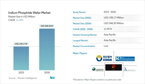
預計 2025 年磷化銦晶片市場規模為 1.9817 億美元,到 2030 年將達到 3.483 億美元,預測期內(2025-2030 年)的複合年成長率為 11.94%。
磷化銦 (InP) 具有可用於生產高效雷射、調變和靈敏檢測器的特性。它還可以產生雷射訊號並將該訊號轉換為電子形式以供識別。這些用於企業網路和資料中心、遠距光纖連接、3G、5G 和 LTE基地台的無線連接以及衛星通訊。這些日益成長的需求正在推動市場的發展。
主要亮點
- 磷化銦晶片擴大被用於汽車雷射雷達、3D感測、消費穿戴設備和通訊領域的資料通訊的成長。預計這將在預測期內推動市場發展。 InPinc 的主要應用還包括 5G通訊、使用光和雷射的資料中心連接、光纖雷射和檢測器、軍事和 5G通訊通訊使用的矽光電、射頻放大器和開關以及健康領域的紅外線熱感成像。
- 被稱為光電裝置的電子元件可以偵測和調節光。光電設備將電資訊轉換為紅外線或可見光能量,反之亦然。光電子技術應用於太陽能發電、光纖通訊系統、監視器和控制電路以及電眼。光電元件用於量子連鎖雷射和受激發射的注入雷射二極體。 LED 和影像感測器用於數位成像系統、包裝和安全應用。
- 根據 2020 年 11 月發布的愛立信移動報告,到 2020 年底,全球行動資料流程量預計將達到每月約 51 EB(Exabyte)。預計到 2026 年,這一數字將成長近 4.5 倍,達到每月 226 EB。這一數字意味著超過 60 億人使用智慧型手機、筆記型電腦和一系列新設備同時消耗行動資料。
- 半導體矽晶圓是電子工業的基礎,也是許多微電子設備的關鍵零件。隨著當前技術、電子設備移動化和數位化的進步,這些物品現在被廣泛應用於各種設備。此外,對更小設備的需求大大增加了對單一設備附加功能的需求,從而推高了矽晶片的價格。
- 新冠疫情導致全球大部分地區實施封鎖,半導體設備產業多種產品的生產陷入停滯。封鎖措施減少了對家用電子電器的需求,影響了全球半導體產業。全球汽車需求和出口出貨量的持續下降對半導體市場產生了負面影響,目前正在減緩半導體製造設備的需求。
磷化銦晶片市場趨勢
消費性電子產品是市場領導者
- 穿戴式科技是一種發展趨勢,它將電子產品融入日常活動,並能夠佩戴在身體的任何部位,以適應不斷變化的生活方式。諸如連接到網際網路以及提供網路和設備之間資料交換選項等趨勢正在引領穿戴式技術的發展趨勢。
- 根據Cisco預測,全球連網穿戴裝置的數量每三年就會加倍,從2016年的3.25億台成長到2019年的7.22億台,預計到2022年將超過10億台。
- 此外,根據日本內務部的數據,截至 2021 年,超過 7% 的日本家庭擁有穿戴式裝置。在整個研究期間(2014-2021年),穿戴式裝置的家庭普及率穩定上升,從2014年的0.5%上升到2020年的5%。
- 全球都市化的不斷上升推動了對先進、美觀的產品的需求,這些產品能夠滿足消費者的需求,例如單一設備中的多種功能和時間表。此外,全球千禧世代是智慧型手錶的早期採用者,因為他們能夠更好地追蹤正常工作時間和奢侈標準消費。
- 例如,根據愛立信的數據,全球智慧型手機用戶數從2020年的59.24億激增至2021年的62.59億。預計2027年將達到76.9億部。
- 此外,根據諾基亞2022年年度行動寬頻指數報告,不斷擴大的4G設備生態系統正在推動4G用戶和資料消費的成長。 2021年,印度智慧型手機出貨量創歷史新高,超過1.6億部,其中包括3000萬部5G設備,其中超過80%的活躍設備支援4G,超過1000萬部活躍的5G設備支援5G。此外,諾基亞的一份報告預測,到 2025 年,智慧型手機普及率將達到 60-75%。
亞太地區可望成為成長最快的市場
- 亞太地區在全球半導體代工市場佔有較大佔有率,擁有台積電、三星電子等巨頭。台灣、韓國、日本和中國在該地區也佔有很大佔有率。根據半導體產業美國(SIA)的數據,從1990年到2020年,美國在全球晶圓廠裝置容量中的佔有率一直在穩步下降。同一時期,亞洲新的半導體工廠快速發展,目前已佔全球產能的相當大一部分。
- 中國有著非常雄心勃勃的半導體計畫。在1500億美元基金的支持下,中國計劃發展國內積體電路產業並生產更多晶片。大中華區(包括中國香港和台灣)是一個地緣政治熱點。美國貿易戰進一步加劇了該地區的緊張局勢,該地區集中了關鍵工藝技術,迫使許多中國公司投資半導體代工廠。
- 中國於2021年3月發布的2021-2025年新五年規劃將加強基礎研究作為重要優先事項。預計2021年中央政府對基礎研究的支出將成長11%,遠高於計畫的整體研發投入7%和6%的GDP成長目標。半導體被認定為七個優先提供資金和資源的領域之一。設計公司開發奈米級積體電路,執行電子設備運作的關鍵任務,包括運算、儲存、網路連接和電源管理。由於晶片需求強勁,預計 2021 年利潤將成長一倍以上。中國領先的半導體代工廠已為 2022 年的產能開發預留了創紀錄的資金。今年,中芯國際已預留了 50 億美元的資本支出,高於 2021 年的 45 億美元。
- 中國在7nm晶片生產方面距離自力更生越來越近。據報道,中國在 7nm 晶片製造流程方面取得了突破,並在製造過程的多個環節開發了工具和技術,以減少對海外設備和材料供應商的依賴。
- 研究和合作的大幅擴展將進一步提高市場成長率。例如,LioniX International (LXI) 和中國科學院微電子研究所 (IMECAS) 已同意透過積極支援能力和提供兩個平台來擴大其光子積體電路 (PIC) 平台夥伴關係。 PIC 的重要平台包括 SOI(絕緣體上矽)、InP(磷化銦)和基於氮化矽的 TriPleX 平台。這些平台可透過多計劃晶圓(MPW)存取取得。
磷化銦晶片產業概況
磷化銦晶片製造領域正在見證領先製造商的不斷增加,預計在預測期內競爭對手之間的競爭將更加激烈。 JX Nippon Mining & Metals 和 Powerway Advanced Materials 等市場現有企業對整個市場產生了相當大的影響。
- 2022 年 3 月:英特爾透露在德國建造第二家晶片製造地(即「大型工廠」)的計畫。此外,2021 年 8 月,ACM Research Inc. 推出了其 Bevel Etch 產品,進一步擴展了 ACM 的綜合濕式工具產品線。該工具最大限度地減少了邊緣污染對後續製程步驟的影響,並提高了晶片製造的產量比率。
- 2022 年 2 月:加拿大政府宣布對加拿大半導體和光電產業進行重大投資。這項 2.4 億加元的投資將鞏固加拿大在光電的全球領先地位,並加強半導體開發和製造。加拿大擁有100多家從事微晶片研發的國內外半導體公司。在化合物半導體、電子機械系統(MEMS)和先進封裝等領域擁有 30 多個應用實驗室和 5 個商業設施。
其他福利:
- Excel 格式的市場預測 (ME) 表
- 3個月的分析師支持
目錄
第1章 引言
- 研究假設和市場定義
- 研究範圍
第2章調查方法
第3章執行摘要
第4章 市場洞察
- 市場概覽
- 產業吸引力-波特五力分析
- 供應商的議價能力
- 買家/消費者的議價能力
- 新進入者的威脅
- 替代品的威脅
- 競爭對手之間的競爭
- 產業價值鏈分析
- 技術簡介
- COVID-19 產業影響評估
第5章市場動態
- 市場促進因素
- 光電設備的使用日益增多
- 資料通訊業務與5G的發展
- 市場限制
- 與其他替代品的競爭
第6章市場區隔
- 依直徑
- 50.8 毫米或 2 英寸
- 76.2毫米或3英寸
- 超過 100 毫米或 4 英寸
- 最終用戶產業應用
- 消費性電子產品
- 通訊設備
- 醫療保健
- 其他最終用戶產業
- 按地區
- 北美洲
- 歐洲
- 亞太地區
- 世界其他地區
第7章競爭格局
- 公司簡介
- AXT Inc.
- Wafer World Inc.
- Logitech Ltd.
- Western Minmetals(SC)Corporation
- Century Goldray Semiconductor Co. Ltd
- Semiconductor Wafer Inc.
- Ding Ten Industrial Inc.
- Sumitomo Electric Semiconductor Materials Inc.(Sumitomo Electric Industries Ltd)
- Xiamen Powerway Advanced Material Co. Ltd
- JX Nippon Mining & Metals Corporation(Eneos Holdings Inc.)
第8章投資分析
第9章 市場機會與未來趨勢
The Indium Phosphide Wafer Market size is estimated at USD 198.17 million in 2025, and is expected to reach USD 348.30 million by 2030, at a CAGR of 11.94% during the forecast period (2025-2030).
Indium phosphide (InP) has properties that produce highly efficient lasers, modulators, and sensitive photodetectors. It can also generate laser signals and convert and identify those signals back to the electronic form. These are used for company networks and data centers, long-haul optical fiber connections over far distances, wireless connections for 3G, 5G, and LTE base stations, and satellite communication. The growth in such requirements is driving the market.
Key Highlights
- Indium phosphide wafers are increasingly adopted in the manufacture of LiDAR for automotive, 3D sensing, consumer wearables, and the growth in datacom in the telecommunication sector. This is expected to drive the market during the forecast period. In addition, some of the major applications of InPinclude 5G communications, data center connectivity that uses lights and lasers, fiber optic lasers and detectors, silicon photonics, RF amplifiers, and switches used in military and 5G communications, and infrared thermal imaging in health.
- Electronic components known as optoelectronic devices detect and regulate light. They convert electrical information into infrared or visible energy and vice versa. It is utilized in photovoltaic power supply, optical fiber communication systems, monitor and control circuits, and electric eyes. Optoelectronic components are used in quantum cascade lasers and injection laser diodes for stimulated emission. LEDs and image sensors are utilized in digital imaging systems, packaging, and safety applications.
- According to the Ericsson Mobility Report published in November 2020, the global mobile data traffic was estimated to reach around 51 EB (exabytes) per month by the end of 2020. This was projected to grow by a factor of almost 4.5 to reach 226 EB per month in 2026. This figure represents the mobile data that will be consumed by greater than 6 billion people using smartphones, laptops, and a multitude of new devices at a time.
- The semiconductor silicon wafer serves as the foundation of the electronics industry and is the main component of many microelectronic devices. With the current advances in the technology landscape, electronic mobility, and digitalization, these items are finding use in a wide range of devices. The requirement for additional capability from a single device has also grown dramatically as a result of the need for small-sized gadgets, which boosts the price of the silicon wafer.
- The COVID-19 pandemic has halted the manufacturing of several items in the semiconductor production equipment industry owing to the continued lockdown in most regions across the world. Lockdown measures reduced the demand for consumer electronic gadgets, which had a global impact on the semiconductor sector. The continued decline in worldwide demand and export shipments for automobiles caused a negative impact on the semiconductor market, which is currently slowing down the demand for semiconductor manufacturing equipment.
Indium Phosphide Wafer Market Trends
Consumer Electronics Segment Expected to Drive the Market
- Wearable technology, a developing trend, integrates electronics into daily activities and addresses the changing lifestyles with the ability to be worn on any part of the body. Factors such as the ability to connect to the internet and provide data exchange options between a network and a device are leading to the trend of wearable technology.
- According to Cisco Systems, the number of connected wearable devices globally has doubled in the span of three years, increasing from 325 million in 2016 to 722 million in 2019. The number of devices is forecasted to be over 1 billion by 2022.
- Further, according to the Ministry of Internal Affairs and Communications (Japan), as of 2021, over 7% of households in Japan owned a wearable device. The household penetration rate of wearable devices steadily increased throughout the surveyed period (2014-2021), rising from 0.5% in 2014 to 5% in 2020.
- The rising rates of urbanization in various parts of the world have driven the demand for advanced, aesthetically appealing products that possess the ability to serve the consumers' requirements better, such as multiple features in one device and time schedules. Moreover, the vast millennial population across the globe has been quick to adopt smartwatches, owing to the increased spending ability on their regular work hours tracking and luxury standards.
- For instance, according to Ericsson, the number of smartphone subscriptions worldwide witnessed an upsurge from 5,924 million in 2020 to 6,259 million in 2021. The number is estimated to reach 7,690 million in 2027.
- Further, according to the Nokia annual mobile broadband index report 2022, the growing ecosystem of 4G-capable devices is driving the growth in 4G subscribers and data consumption. India recorded the highest-ever shipment of over 160 million smartphones, including 30 million 5G devices, in 2021, with active 4G capable devices crossing 80% and the number of active 5G capable devices crossing 10 million. The Nokia report also forecasted that user adoption will increase to 60-75% of the smartphone user base by 2025.
Asia-Pacific Expected to be the Fastest-growing Market
- The Asia-Pacific region commands a prominent share of semiconductor foundries globally, with major companies such as TSMC and Samsung Electronics. Taiwan, South Korea, Japan, and China have a significant market share in the region. According to the US Semiconductor Industry Association (SIA), the US share of the global installed wafer fab capacity constantly declined from 1990 to 2020. During the same period, Asia saw a meteoric rise in developing new fabs to the point where it now accounts for a significant share of the world's capacity.
- China has a very ambitious semiconductor agenda. Backed by USD 150 billion in funding, the country is developing its domestic IC industry and plans to make more of its chips. Greater China, which encompasses Hong Kong, China, and Taiwan, is a geopolitical hotspot. The US-China trade war is compounding tensions in an area where all the leading process technology is located, forcing many Chinese companies to invest in their semiconductor foundries.
- China's new five-year plan for 2021-2025, announced in March 2021, established that boosting basic research was a critical priority. The central government's spending on basic research was expected to increase by 11% in 2021, well above the 7% planned for the overall R&D investment and the 6% target for GDP growth. Semiconductors were designated as one of the seven areas that will be given priority in terms of funding and resources. Firms involved in design develop nanometer-scale integrated circuits that perform the critical tasks that make electronic devices work, such as computing, storage, network connectivity, and power management. The profit was estimated to more than double in 2021 because of the robust chip demand. China's leading semiconductor foundry set aside a record sum for capacity development in 2022. This year, Semiconductor Manufacturing International Corp (SMIC) set aside USD 5 billion for capital spending, up from USD 4.5 billion in 2021.
- China is moving significantly closer to self-reliance in 7 nm chip production. China has made breakthroughs in its 7 nm chip-making process, reportedly developing tools and know-hows for several segments of the manufacturing process amid efforts to reduce reliance on foreign equipment and material vendors.
- The significant research and partnership growth further bolsters the market growth rate. For instance, LioniXInternational (LXI) and the Institute of Microelectronics Chinese Academy of Science (IMECAS) agreed to expand their Photonic Integrated Circuit (PIC) platform partnership by actively supporting the functionality and offering both platforms. The critical platforms in the PIC landscape include Silicon On Insulator (SOI), Indium Phosphide (InP), and the silicon nitride-based TriPleXplatform. These platforms are available through Multi-Project Wafer (MPW) access.
Indium Phosphide Wafer Industry Overview
The growing presence of large manufacturers in the indium phosphide wafer manufacturing sector is expected to intensify competitive rivalry during the forecast period. Market incumbents, such as JX Nippon Mining & Metals Corporation and Powerway Advanced Material Co. Ltd, considerably influence the overall market.
- March 2022: Intel revealed plans for a second new 'Megafab," a chipmaking site in Germany, with an expected USD 88 billion in investments across several European countries. Further, in August 2021, ACM Research Inc. launched its Bevel Etch product, which further expanded ACM's comprehensive offering of wet tools. This tool minimizes the impact of edge contamination for subsequent process steps and improves chip manufacturing yield.
- February 2022: The Government of Canada announced a significant investment in the Canadian semiconductor and photonics industries. The investment of CAD 240 million will help solidify Canada's role as a global leader in photonics and will bolster the development and manufacturing of semiconductors. Over 100 domestic and international semiconductor companies work on microchip research and development in Canada. There are over 30 applied research laboratories and five commercial facilities for areas including compound semiconductors, microelectromechanical systems (MEMS), and advanced packaging.
Additional Benefits:
- The market estimate (ME) sheet in Excel format
- 3 months of analyst support
TABLE OF CONTENTS
1 INTRODUCTION
- 1.1 Study Assumptions and Market Definition
- 1.2 Scope of the Study
2 RESEARCH METHODOLOGY
3 EXECUTIVE SUMMARY
4 MARKET INSIGHTS
- 4.1 Market Overview
- 4.2 Industry Attractiveness - Porter's Five Forces Analysis
- 4.2.1 Bargaining Power of Suppliers
- 4.2.2 Bargaining Power of Buyers/Consumers
- 4.2.3 Threat of New Entrants
- 4.2.4 Threat of Substitute Products
- 4.2.5 Intensity of Competitive Rivalry
- 4.3 Industry Value Chain Analysis
- 4.4 Technology Snapshot
- 4.5 Assessment of the Impact of COVID-19 on the Industry
5 MARKET DYNAMICS
- 5.1 Market Drivers
- 5.1.1 Increasing Use of Optoelectronic Devices
- 5.1.2 Growth of Datacom Business and 5G
- 5.2 Market Restraints
- 5.2.1 Competition from Other Substitutes
6 MARKET SEGMENTATION
- 6.1 By Diameter
- 6.1.1 50.8 mm or 2 "
- 6.1.2 76.2 mm or 3 "
- 6.1.3 100 mm or 4" and Above
- 6.2 By End-user Industry Application
- 6.2.1 Consumer Electronics
- 6.2.2 Telecommunications
- 6.2.3 Medical
- 6.2.4 Other End-user Industry Applications
- 6.3 By Geography
- 6.3.1 North America
- 6.3.2 Europe
- 6.3.3 Asia-Pacific
- 6.3.4 Rest of the world
7 COMPETITIVE LANDSCAPE
- 7.1 Company Profiles
- 7.1.1 AXT Inc.
- 7.1.2 Wafer World Inc.
- 7.1.3 Logitech Ltd.
- 7.1.4 Western Minmetals (SC) Corporation
- 7.1.5 Century Goldray Semiconductor Co. Ltd
- 7.1.6 Semiconductor Wafer Inc.
- 7.1.7 Ding Ten Industrial Inc.
- 7.1.8 Sumitomo Electric Semiconductor Materials Inc. (Sumitomo Electric Industries Ltd)
- 7.1.9 Xiamen Powerway Advanced Material Co. Ltd
- 7.1.10 JX Nippon Mining & Metals Corporation (Eneos Holdings Inc.)
8 INVESTMENT ANALYSIS
9 MARKET OPPORTUNITIES AND FUTURE TRENDS
 GaAS晶圓市場-全球產業規模、佔有率、趨勢、機會及預測,依產品類型(LEC生長GaAS、VGF生長GaAS及其他)、產品應用(射頻、LED、VCSEL、光伏)、地區及競爭格局分類,2020-2030年預測
 磷化銦晶片市場-2025-2030年預測
 砷化鎵晶片市場按應用、摻雜、直徑、晶片類型和銷售管道分類-2025-2032年全球預測半導體晶圓分選系統市場(依設備類型、分選技術、類別和最終用戶)-2025-2030 年全球預測
 晶圓溫度測量系統的全球市場全球磷化銦晶片市場規模(按類型、應用、區域範圍和預測)拋光矽晶圓市場:未來預測(2025-2030)
 砷化鎵 (GaAs) 晶片:市場佔有率分析、產業趨勢和成長預測(2025-2030 年)AAO晶圓市場:現況分析與預測(2024-2032)
 全球陽極氧化鋁晶圓市場規模研究,按晶圓類型(6 吋、8 吋、12 吋等)、應用(消費性電子、製藥、工業、其他)和 2022-2032 年區域預測