


 |
市場調查報告書
商品編碼
1407943
高階半導體封裝:市場佔有率分析、產業趨勢與統計、2024年至2029年成長預測High-end Semiconductor Packaging - Market Share Analysis, Industry Trends & Statistics, Growth Forecasts 2024 - 2029 |
||||||
※ 本網頁內容可能與最新版本有所差異。詳細情況請與我們聯繫。
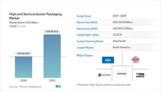
高階半導體封裝市場規模預計到2024年為369.5億美元,預計到2029年將達到859.1億美元,在預測期內(2024-2029年)複合年成長率為15.10%。
封裝擴大用於提高電子系統的性能、可靠性和成本效益,並且在行業內各個終端用戶垂直領域的需求量很大,從而導致整合度、能源效率和產品性能的不斷發展正在加速市場成長。例如,2022年3月,英特爾鏈在歐盟半導體價值鏈上投資了800億歐元,其中包括尖端封裝技術。
主要亮點
- 包裝可保護電子系統免受高頻噪音輻射、靜電放電、機械損壞和冷卻的影響。全球半導體產業的成長是推動半導體封裝市場成長的關鍵因素之一。此外,2023年2月,半導體產業協會(SIA)宣布,2022年全球半導體產業銷售額將達到5,741億美元,創歷史最高年度總合,較上年公佈的5,559億美元成長3.3%。
- 此外,物聯網、人工智慧的興起以及複雜電子設備的普及正在推動消費性電子和汽車產業的高階應用。由於這些因素,正在採用更先進的半導體封裝技術來維持需求。
- 此外,2022年6月,代表歐洲整個電子製造和設計供應鏈的組織SEMI Europe呼籲儘早通過《歐洲晶片法》,並邀請歐盟委員會、成員國和議會討論法案。參與。該法律旨在增強歐洲在半導體技術和應用方面的競爭力和彈性,同時支持該地區向數位和綠色經濟轉型。
- 該領域研究活動的活性化進一步刺激了市場需求。例如,德累斯頓已發展成為著名的半導體研究中心。 2022 年 6 月,Fraunhofer IPMS 和 IZM-ASSID 宣布合作建立薩克森高級 CMOS 和異質整合中心。該中心將提供整個300毫米微電子價值鏈,並需要高科技研究來實現未來的創新。
- Fraunhofer IPMS在無塵室設備上投資超過1.4億歐元,在CMOS製造前端的現代300毫米晶圓行業標準的應用研究方面在德國擁有強大的地位。 Fraunhofer IZM-ASSID 提供的創新封裝和系統整合技術補充了這項知識。
- 此外,由於 5G、物聯網、汽車和 HPC 等多個長期成長促進因素,半導體封裝市場預計將擴大。例如,印度政府最近核准了一項100億美元的獎勵計劃,以建立一個完整的半導體生態系統,包括晶圓廠、本土晶片設計和化合物半導體工廠。
- 此外,俄羅斯和烏克蘭之間持續的衝突預計將對電子產業產生重大影響。這場衝突已經加劇了已經影響該行業的半導體供應鏈問題和晶片短缺問題。這種干擾可能會表現為鎳、鈀、銅、鈦、鋁和鐵礦石等關鍵原料的價格波動,從而導致材料短缺。這可能會成為所研究市場的製造障礙。
高階半導體封裝市場趨勢
消費性電子產業可望提振市場
- 消費性電子部門正在半導體封裝市場進行大量投資。智慧型手機的成長、穿戴式裝置和智慧型裝置的普及不斷提高,以及消費者物聯網裝置在智慧家庭等應用中的普及不斷提高,是影響該細分市場成長的一些因素。愛立信預計,2022年全球智慧型手機行動網路用戶數量預計將達到約66億,2028年將超過78億人。
- 此外,由於複雜的半導體元件可以提供越來越多的功能和特性,智慧型手錶和智慧揚聲器市場近年來變得非常受歡迎。因此,對Wi-Fi和藍牙晶片的需求急劇增加。消費性電子製造商也利用半導體元件為其產品配備物聯網和人工智慧模型,以改善用戶體驗並為產品增添光彩。
- 例如,2023年3月,華為計畫在未來幾年推出一款電池大幅升級的折疊式智慧型手機。據傳該設備將進行電池升級並命名為「Mate X3」。此外,華為很可能會採用高矽負極材料來增強智慧型手機的電池容量,預計達到5060mAh。
- 電腦和筆記型電腦現已成為大力投資科技的年輕消費者的必需品。此外,電子產業的創新和進步預計將在未來十年推動半導體封裝銷售。由於物聯網和人工智慧的引入,全球新興市場和已開發市場的半導體封裝銷售額預計將增加。
- 2022年6月,英特爾公司與倫敦大學學院(UCL)聯合發布了一款新型非接觸式電腦,可以透過手、頭、臉和全身的手勢進行操作和控制。電子市場不斷要求更高的功耗、更快的速度、更多的引腳數、更小的佔地面積和更薄的設計。半導體的小型化和整合化正在創造更輕、更小、更攜帶的家用電器,例如智慧型手機、平板電腦和新興的物聯網設備。
北美市場正在經歷顯著成長
- 美國和加拿大的半導體產業在人工智慧、量子運算和 5G 等先進無線網路等未來關鍵技術中保持著重要地位。例如,根據GSMA的預測,2025年5G將成為美國領先的網路技術。 5G 網路的持續部署與對更即時和高效能運算設備的需求不斷成長相一致,其中半導體是其中的關鍵要素。
- 美國政府正在進行重大投資,以促進先進技術的普及,從而增強對高階半導體封裝的需求。美國是世界上成長最快的經濟體之一。根據 WSTS 數據,2022 年 10 月美洲半導體銷售額為 122.9 億美元,高於上月的 120.3 億美元。
- 美國參議院最近宣布了促進美國製造半導體(FABS)法案。該法案可為半導體製造設備和製造工廠的投資提供 25% 的投資稅額扣抵。
- 此外,2022年9月,拜登政府宣布將加強國內半導體產業,以對抗對中國的依賴,因為美國消耗了全球25%的最先進晶片,這些晶片對國家安全至關重要,且產量為零。將投資500億美元發展拜登總統於 2022 年 8 月簽署了 2800 億美元的 CHIPS 法案,以促進國內高科技製造業,作為增強美國對中國競爭力的努力的一部分。該地區半導體行業如此強勁的投資可能會為研究市場的成長提供利潤豐厚的機會。
- 此外,美國是最大的電動車市場之一,近年來電動車銷量激增。據 KBB 稱,2022 年第二季度美國售出近 196,800 輛純電動車。與去年同期相比成長約66.4%。
- 近年來,美國實施了許多法規來促進電動車的普及。例如,紐約州立法機關最近通過了一項法案,實際上要求到 2035 年該州銷售的所有新小客車都必須採用電力驅動。此外,美國也制定了2030年該國銷售的汽車一半為電動車的目標。
高階半導體封裝產業概況
高階半導體封裝市場正在整合。公司正在利用產品創新、擴張和聯盟來在競爭中生存並擴大市場範圍。
2022年10月,台積電宣布成立開放創新平台(OIP)3D Fabric聯盟。最新的台積電 3D Fabric 聯盟是台積電的第六個 OIP 聯盟,為半導體設計、內存模組、測試、製造、基板技術和封裝提供全面的一流解決方案和服務,包括 3D IC半導體公司的同類聯盟與合作夥伴合作,加速生態系統的準備與創新。
2022 年 8 月,英特爾公佈了其最新的架構和封裝突破,可實現基於 2.5D 和 3D 區塊的晶片設計,開創了晶片製造技術和影響的新時代。英特爾的系統代工模式以封裝改進為特色,該公司計劃在 2030 年將封裝上的電晶體數量從 1,000 億個增加到 1 兆個。
其他福利:
- Excel 格式的市場預測 (ME) 表
- 3 個月的分析師支持
目錄
第1章簡介
- 研究假設和市場定義
- 調查範圍
第2章調查方法
第3章執行摘要
第4章市場洞察
- 市場概況
- 產業吸引力-波特五力分析
- 供應商的議價能力
- 買方議價能力
- 新進入者的威脅
- 替代品的威脅
- 競爭公司之間敵對關係的強度
- 產業價值鏈分析
- 評估宏觀經濟趨勢對市場的影響
第5章市場動態
- 市場促進因素
- 各行業半導體元件消費擴大
- 擴大 3D 列印在半導體封裝的應用
- 市場抑制因素
- 半導體IC設計初始投資高、複雜
第6章市場區隔
- 依技術
- 3D SoC
- 3D堆疊內存
- 2.5D中介層
- UHD FO
- 內置矽橋
- 按最終用戶
- 消費性電子產品
- 航太/國防
- 醫療設備
- 電訊
- 車
- 其他最終用戶
- 按地區
- 北美洲
- 美國
- 加拿大
- 歐洲
- 英國
- 德國
- 法國
- 義大利
- 其他歐洲國家
- 亞太地區
- 中國
- 印度
- 日本
- 澳洲
- 東南亞
- 其他亞太地區
- 世界其他地區
- 北美洲
第7章競爭形勢
- 公司簡介
- Intel Corporation
- Taiwan Semiconductor Manufacturing Company
- Advanced Semiconductor Engineering, Inc.
- Samsung Electronics Co. Ltd
- Amkor Technology Inc.
- JCET Group Co., Ltd.
- TongFu Microelectronics Co., Ltd.
- Fujitsu Limited
- Siliconware Precision Industries Co. Ltd
- Powertech Technology, Inc.
第8章投資分析
第9章市場的未來
The High-end Semiconductor Packaging Market size is estimated at USD 36.95 billion in 2024, and is expected to reach USD 85.91 billion by 2029, growing at a CAGR of 15.10% during the forecast period (2024-2029).
The continuous advancements in integration, energy efficiency, and product characteristics because of the growing demand across various end-user verticals of the industry and the use of packaging for improving the performance, reliability, and cost-effectiveness of electronic systems accelerate the market's growth. For instance, in March 2022, Intel Corp. invested EUR 80 billion across the entire semiconductor value chain in the European Union, including cutting-edge packaging technologies.
Key Highlights
- Packaging protects an electronic system from radio frequency noise emission, electrostatic discharge, mechanical damage, and cooling. The rise in the semiconductor industry worldwide is one of the major factors driving the growth of the semiconductor packaging market. In addition, in February 2023, the Semiconductor Industry Association (SIA) announced global semiconductor industry sales totaled USD 574.1 billion in 2022, the highest-ever annual total and an increase of 3.3% compared to the previous year's total of USD 555.9 billion.
- Furthermore, the rise of IoT and AI and the proliferation of complex electronics drive the high-end application segment in the consumer electronics and automotive industries. Due to these factors, more advanced semiconductor packaging technologies are being adopted to sustain demand.
- Further, in June 2022, SEMI Europe, the organization representing the entire European electronics manufacturing and design supply chain, immediately called for the quick passage of the European Chips Act and invited the European Commission, Member States, and Parliament to participate in discussions about the proposed legislation. The Act intends to support the region's transition to a digital and green economy while enhancing Europe's competitiveness and resilience in semiconductor technologies and applications.
- The growing research activities in the sector further bolstered the market's demand. For instance, Dresden is developing into a renowned hub for semiconductor research. In June 2022, Fraunhofer IPMS and IZM-ASSID announced a collaboration to form the Center for Advanced CMOS & Heterointegration Saxony. The center will provide the entire 300 mm microelectronics value chain, requiring high-tech research for upcoming innovations.
- Fraunhofer IPMS is positioned in Germany in applied research on the contemporary 300mm wafer industry standard in the front end of CMOS manufacturing, having recently invested over EUR 140 million in clean room equipment. Innovative packaging and system integration technologies from Fraunhofer IZM-ASSID supplement this knowledge.
- Furthermore, the semiconductor packaging market is expected to expand due to multiple long-term growth drivers, like 5G, IoT, automotive, and HPC. For instance, the government of India recently approved a USD 10 billion incentive package to build a complete semiconductor ecosystem, including fabs, home-grown chip design, and compound semiconductor plants.
- Moreover, the ongoing conflict between Russia and Ukraine is expected to impact the electronics industry significantly. The conflict has already exacerbated the semiconductor supply chain issues and the chip shortage that have affected the industry for some time. The disruption may come in the form of volatile pricing for critical raw materials such as nickel, palladium, copper, titanium, aluminum, and iron ore, resulting in material shortages. This would obstruct manufacturing in the studied market.
High-end Semiconductor Packaging Market Trends
Consumer Electronics Sector is Expected to Boost the Market
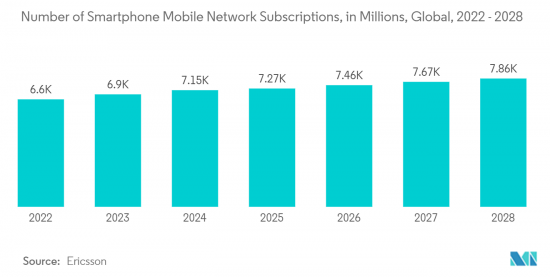
- The consumer electronics sector is significantly investing in the semiconductor packaging market. Growth of the smartphone, rising wearable and smart device adoption, and increasing consumer IoT device penetration in applications like smart homes are a few of the influential factors influencing the segment's growth. According to Ericsson, smartphone mobile network subscriptions worldwide reached nearly 6.6 billion in 2022 and are predicted to exceed 7.8 billion by 2028.
- Additionally, markets for smartwatches and smart speakers have become extremely popular in recent years due to the growing number of features and functionalities they can offer due to sophisticated semiconductor components. As a result, demand for Wi-Fi and Bluetooth chips increased dramatically. Consumer electronics manufacturers also use semiconductor components to equip their products with IoT and AI models, enhancing user experience and making products brighter.
- For instance, in March 2023, Huawei planned to launch its foldable smartphone with a significant battery upgrade in the coming years. The device will feature an upgrade to its battery, and it is rumored to be named the Mate X3. Further, Huawei will likely use the high-silicon anode material to enhance the smartphone's battery capacity, which is expected to be 5060mAh.
- Personal computers and laptops are now essential for young consumers heavily invested in technology. In addition, over the next ten years, innovation and advancement in the electronics sector are anticipated to drive semiconductor packaging sales. Sales of semiconductor packaging are expected to increase globally in both developing and developed markets due to the introduction of IoT and AI.
- Intel Corporation and the University College London (UCL) collaborated in June 2022 to introduce a new touchless computer that can be operated and controlled by gesturing the hands, head, face, and entire body. Higher power dissipation, faster speeds, higher pin counts, smaller footprints, and lower profiles are all constant demands in the electronics market. Semiconductor miniaturization and integration have resulted in lighter, smaller, and more portable appliances such as smartphones, tablets, and emerging IoT devices.
North America to Experience Significant Market Growth
- The semiconductor sector in the United States and Canada has maintained a significant position in key future technologies, such as AI, quantum computing, and sophisticated wireless networks like 5G. For instance, as per GSMA, 5G will become the lead network technology in the US by 2025. The increasing implementation of 5G networks coincides with the growing demand for more immediate high-performance computing appliances, for which semiconductors form a critical element.
- The United States Government has significantly invested in boosting the penetration of advanced technologies, bolstering the demand for high-end semiconductor packaging. The United States is one of the world's fastest-expanding economies. According to WSTS, in October 2022, semiconductor sales in the Americas amounted to USD 12.29 billion, an increase from the USD 12.03 billion recorded for the previous month.
- The US Senate recently announced the Facilitating American-Built Semiconductors (FABS) Act, which may provide tax incentives to semiconductor manufacturers. The bill may establish a 25% investment tax credit for semiconductor manufacturing investments in equipment or fabs.
- Additionally, in September 2022, the Biden administration announced that it would invest USD 50 billion in building up the domestic semiconductor industry to counter dependency on China, as the US produces zero and consumes 25% of the world's leading-edge chips vital for its national security. President Joe Biden signed a USD 280 billion CHIPS bill in August 2022 to boost domestic high-tech manufacturing, part of his administration's push to increase US competitiveness over China. Such robust investments in the semiconductor sector in the region would offer lucrative opportunities for the growth of the studied Market.
- Furthermore, the United States is one of the largest markets for electric vehicles, and the country has also recorded rapid growth in EV sales in recent years. According to KBB, in the Q2 of 2022, just under 196,800 battery electric cars were sold in the United States. This was a year-over-year boost of around 66.4% compared to the sales recorded in Q2 of the previous year.
- Many regulations have been implemented in recent years to promote the use of electric vehicles in the country. For instance, New York state lawmakers recently passed a bill that essentially mandates that all new passenger cars sold in the state run on electric power by 2035. Moreover, the United States has set a target to ensure half of the vehicles sold in the country are electric by 2030.
High-end Semiconductor Packaging Industry Overview
The market for high-end semiconductor packaging is consolidated. Companies employ product innovation, expansions, and partnerships to stay ahead of the competition and widen their market reach. Several recent market developments include:
In October 2022, TSMC announced the Open Innovation Platform (OIP) 3D Fabric Alliance. The latest TSMC 3DFabric Alliance is TSMC's sixth OIP Alliance and the first of its variety in the semiconductor firm that joins forces with partners to accelerate 3D IC ecosystem readiness and innovation, with an entire expanse of best-in-class solutions and services for semiconductor design, memory modules, testing, manufacturing, substrate technology, and packaging.
In August 2022, Intel showcased the most recent architectural and packaging breakthroughs that enabled 2.5D and 3D tile-based chip designs, ushering in a new era in chipmaking technologies and their significance. Intel's system foundry model features improved packaging, and the company intends to increase the number of transistors on a package from 100 billion to 1 trillion by 2030.
Additional Benefits:
- The market estimate (ME) sheet in Excel format
- 3 months of analyst support
TABLE OF CONTENTS
1 INTRODUCTION
- 1.1 Study Assumptions and Market Definitions
- 1.2 Scope of the Study
2 RESEARCH METHODOLOGY
3 EXECUTIVE SUMMARY
4 MARKET INSIGHTS
- 4.1 Market Overview
- 4.2 Industry Attractiveness - Porter's Five Forces Analysis
- 4.2.1 Bargaining Power of Suppliers
- 4.2.2 Bargaining Power of Buyers
- 4.2.3 Threat of New Entrants
- 4.2.4 Threat of Substitute Products
- 4.2.5 Intensity of Competitive Rivalry
- 4.3 Industry Value Chain Analysis
- 4.4 Assessment of the Impact of Macroeconomic Trends on the Market
5 MARKET DYNAMICS
- 5.1 Market Drivers
- 5.1.1 Growing Consumption of Semiconductor Devices Across Industries
- 5.1.2 Growing adoption of 3D printing in semiconductor packaging
- 5.2 Market Restraints
- 5.2.1 High Initial Investment and Increasing Complexity of Semiconductor IC Designs
6 MARKET SEGMENTATION
- 6.1 By Technology
- 6.1.1 3D SoC
- 6.1.2 3D Stacked Memory
- 6.1.3 2.5D interposers
- 6.1.4 UHD FO
- 6.1.5 Embedded Si Bridge
- 6.2 By End-users
- 6.2.1 Consumer Electronics
- 6.2.2 Aerospace and Defense
- 6.2.3 Medical Devices
- 6.2.4 Telecom and Communication
- 6.2.5 Automotive
- 6.2.6 Other End-users
- 6.3 By Geography
- 6.3.1 North America
- 6.3.1.1 U.S.
- 6.3.1.2 Canada
- 6.3.2 Europe
- 6.3.2.1 United Kingdom
- 6.3.2.2 Germany
- 6.3.2.3 France
- 6.3.2.4 Italy
- 6.3.2.5 Rest of Europe
- 6.3.3 Asia-Pacific
- 6.3.3.1 China
- 6.3.3.2 India
- 6.3.3.3 Japan
- 6.3.3.4 Australia
- 6.3.3.5 South East Asia
- 6.3.3.6 Rest of Asia-Pacific
- 6.3.4 Rest of the World
- 6.3.1 North America
7 COMPETITIVE LANDSCAPE
- 7.1 Company Profiles
- 7.1.1 Intel Corporation
- 7.1.2 Taiwan Semiconductor Manufacturing Company
- 7.1.3 Advanced Semiconductor Engineering, Inc.
- 7.1.4 Samsung Electronics Co. Ltd
- 7.1.5 Amkor Technology Inc.
- 7.1.6 JCET Group Co., Ltd.
- 7.1.7 TongFu Microelectronics Co., Ltd.
- 7.1.8 Fujitsu Limited
- 7.1.9 Siliconware Precision Industries Co. Ltd
- 7.1.10 Powertech Technology, Inc.
8 INVESTMENTS ANALYSIS
9 FUTURE OF THE MARKET
 高密度實裝(MCM,MCP,SIP,3D-TSV):市場分析及技術趨勢
 2024-2028年全球高階半導體封裝市場
 2024-2032 年半導體封裝市場報告(按類型、封裝材料、技術、最終用戶和地區)
 2.5D 和 3D 半導體封裝 - 市場佔有率分析、產業趨勢與統計、成長預測(2024 - 2029)
 面板級封裝:市場佔有率分析、產業趨勢與統計、成長預測(2024-2029)
 全球半導體封裝市場規模、佔有率、成長分析(按材料、按應用)- 2023-2030 年產業預測
 2024 年 3D 半導體封裝全球市場報告
 先進半導體封裝市場報告:2030 年趨勢、預測與競爭分析
 嵌入式晶片封裝市場報告:2030 年趨勢、預測與競爭分析
 面板級封裝報告:2030 年趨勢、預測與競爭分析