


 |
市場調查報告書
商品編碼
1406092
半導體測量與檢測設備:市場佔有率分析、產業趨勢、2024年至2029年成長預測Semiconductor Metrology And Inspection Equipment - Market Share Analysis, Industry Trends & Statistics, Growth Forecasts 2024 - 2029 |
||||||
※ 本網頁內容可能與最新版本有所差異。詳細情況請與我們聯繫。
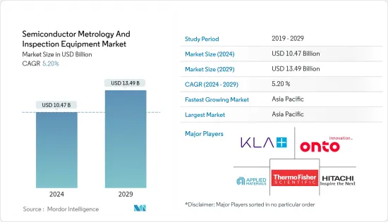
預計2024年半導體計量及檢測設備市場規模為104.7億美元,預計2029年將達到134.9億美元,預測期間(2024-2029年)複合年成長率為5.20%。
主要亮點
- 半導體計量和檢測對於管理半導體製造流程至關重要。半導體晶圓的製造過程大約涉及 400 到 600 個步驟,需要一到兩個月的時間。如果在流程早期出現缺陷,那麼流程後期所做的所有工作都將被浪費。在半導體製造過程的重要環節,有測量和檢查過程來確認和維持特定的產量比率。
- 智慧型手機、家用電子電器和汽車應用等應用正在推動對高性能、低成本半導體材料的需求。無線技術(5G)和人工智慧等技術變革正在刺激這些產業。此外,物聯網(IoT)設備的成長趨勢預計將鼓勵半導體產業投資該設備以實現智慧產品。
- 工業和住宅領域互聯物連網型設備的日益普及趨勢增加了對高性能半導體的需求,這反過來又為所研究市場的成長創造了良好的前景。據愛立信稱,到2022年終,連接物聯網技術NB-IoT和Cat-M的設備數量將達到近5億。此外,寬頻物聯網 (4G/5G) 連線預計到 2022 年將達到 13 億,到 2028 年約佔所有蜂巢式物聯網連線的 60%。
- 然而,高設置成本和缺乏處理測量系統的專業知識等因素預計將有效阻礙預測期內的市場成長。為了應對這些課題,服務型企業正在依需提供計量服務,使他們能夠在精密尺寸測量的專業領域提供專業的擴展。
- 此外,當前美國貿易爭端等宏觀經濟因素也推動了研究市場,美國對中國實施了多項制裁,並阻止中國獲得先進的半導體設備,這對成長構成課題。由於中國是市場供應鏈的關鍵地區之一,這種趨勢將阻礙市場的成長。
半導體測量和檢測設備市場的趨勢
晶圓檢測取得顯著成長
- 預計3D幾年推動晶圓檢測需求的主要因素之一將是需求的增加。 3D 電路在行動消費性電子產品、感測器、MEMS 和工業產品等多種空間受限的應用中變得越來越流行,因為它們提高了整體產品性能,包括速度、耐用性、更低的功耗和更輕的普及。
- 隨著經濟實惠的雲端處理解決方案的廣泛普及,隨著企業和產業擴大使用伺服器和資料中心系統,微處理器和數位訊號處理器等邏輯裝置變得越來越受歡迎,需求預計將增加。此外,隨著越來越多的連接設備具有物聯網功能,連網型變得越來越普遍。這些設備擴大使用薄晶圓來實現高效的溫度控制並提高性能。所有這些原因都在推動晶圓檢測市場的擴張。
- 由於 300mm 晶圓具有高產量比率,因此在 LED 應用中的快速使用正在推動薄晶圓檢測市場的全球擴張。 300mm 晶圓帶來的規模經濟和盈利能力的提高對於 LED 製造商來說至關重要。隨著300mm晶圓運作設施數量的增加,預計300mm晶圓的需求也將大幅增加。
- 印度在縮小數位付款落差方面正在取得巨大進展。財政部目前建議銀行發行具有近場通訊功能的非接觸式信用卡和簽帳金融卡的指令預計將成為正確方向的催化劑。這些因素預計將推動智慧卡中 RFID 等無線技術的使用,創造對薄晶圓的需求,並推進市場研究。
- 晶圓生產廠的不斷擴張為國內外晶圓檢測廠商根據客戶要求開發新產品創造了機會。例如,根據SEMI的數據,2022年全球矽晶圓面積出貨量達到147.1億平方英寸,高於2021年的141.6億平方英吋。矽晶圓是半導體的關鍵組成部分,展示了高性能半導體在連網型設備中的使用並推動了市場發展。此外,2022年全球矽晶圓總銷售額為138億美元,高於126億美元,進一步反映了市場的成長。
亞太地區主導市場
- 亞太地區是半導體產業製造和消費的重要地區之一。根據SIA統計,亞太地區是最大的半導體市場,其中中國佔最大佔有率。
- 許多地區公司在半導體計量和檢測設備市場建立了聯盟和合作夥伴關係。例如,中國晶片製造工具製造商深圳精拓自動化設備有限公司宣布與中國最大的晶片開發商華為旗下海思半導體簽署了一份為期五年(2021-2025)具有法律約束力的合作備忘錄。兩家公司的目標是擴大在半導體封裝工具開發方面的合作夥伴關係,並創建一個自給自足且不受監管的行業。
- 近年來,亞太地區一直是半導體設備不斷成長的市場。例如,根據 SEMI 的數據,2022 年中國仍是半導體設備的最大支出國,申請達 283 億美元。然而,美國和中國之間的貿易問題正在為半導體計量和檢測設備市場帶來不確定性。國內半導體公司正在大力投資,透過提高產能、轉移技術節點和晶圓尺寸來維持當前的市場地位。未來,預計該地區鑄造廠的需求將會增加。
- 地方政府發展當地半導體產業的措施也為所研究市場的成長創造了良好的前景。例如,中國國務院《國家積體電路產業發展指南》的目標是到2030年使中國在半導體產業的所有領域都處於世界領先地位。此外,「中國製造2025」計劃將先進半導體製造知識作為中國未來經濟的重要組成部分。這項措施高度關注建立強大的國家製造策略。
- 該舉措預計也將鼓勵國內外企業投資包括積體電路在內的半導體製造各個領域。該舉措敦促政府機構加強研發活動,以便中國能夠依靠國內公司而不是外國公司來獲得核心技術。這將促進半導體製造業的創新。
半導體測量和檢測設備產業概況
半導體計量和檢測設備市場的主要參與者包括應用材料公司、尼康計量公司和 KLA 公司。這些公司透過專注於市場擴張和收購來不斷擴大業務。收購活動有效地推動了所研究市場的整體市場成長。大公司也投入大量資源進行研發營運,以保護其市場地位並推動其研究市場的創新。整體而言,競爭程度仍然很高,這主要是由於研究市場中主要企業的強勢存在。
- 2023 年 7 月,先進封裝宣布推出使用混合鍵結和矽穿孔電極(TSV) 將小晶片整合到先進 2.5D 和 3D 封裝中的材料、技術和系統。這項新解決方案擴展了業界領先的異質整合 (HI) 技術的廣度。該公司是最大的HI技術供應商,擁有最佳化的晶片製造系統,涵蓋蝕刻、物理和化學氣相沉積(PVD)、電鍍、化學機械拋光(CMP)、退火和表面處理。
- 2023 年 5 月,KLA Corporation 宣布與imec 建立策略合作夥伴關係,共同開發人才庫和基礎設施,以加速自動駕駛、電動和先進半導體應用,從而推動汽車產業的發展。透過此次合作,雙方將為汽車產業的專案識別和管理、人才開發和招募提供相關專業知識。
其他福利
- Excel 格式的市場預測 (ME) 表
- 3 個月的分析師支持
目錄
第1章簡介
- 研究假設和市場定義
- 調查範圍
第2章調查方法
第3章執行摘要
第4章市場洞察
- 市場概況
- 產業吸引力-波特五力分析
- 供應商的議價能力
- 買方議價能力
- 新進入者的威脅
- 替代品的威脅
- 競爭程度
- 評估主要宏觀趨勢的影響
第5章市場動態
- 市場促進因素
- 對高性能、低成本半導體的需求不斷成長
- 消費性電子產品對半導體晶圓的需求增加
- 市場抑制因素
- 設置成本高且缺乏有效處理測量系統的專業知識
- 原料和製造成本高
第6章市場區隔
- 依類型
- 光刻計量
- 覆蓋
- 尺寸測量裝置
- 掩模檢查/測量
- 晶圓檢查
- 薄膜測量
- 其他過程控制系統
- 光刻計量
- 依地區
- 北美洲
- 歐洲
- 亞太地區
- 世界其他地區
第7章 競爭形勢
- 公司簡介
- KLA Corporation
- Applied Materials Inc.
- Onto Innovation Inc.
- Thermo Fisher Scientific Inc.
- Hitachi Hi-Technologies Corporation(Hitachi Limited)
- Nova Measuring Instruments Ltd
- ASML Holding NV
- Lasertec CorporatioN
- JEOL Ltd
- Nikon Metrology NV(Nikon Group)
- Camtek Limited
第8章投資分析
第9章市場的未來
The Semiconductor Metrology And Inspection Equipment Market size is estimated at USD 10.47 billion in 2024, and is expected to reach USD 13.49 billion by 2029, growing at a CAGR of 5.20% during the forecast period (2024-2029).
Key Highlights
- Semiconductor metrology and inspection are essential for managing the semiconductor manufacturing process. There are about 400 to 600 steps in the manufacturing process of semiconductor wafers, which are undertaken in one to two months. If deficiencies occur early in the process, all the work undertaken in the subsequent steps will be wasted. Metrology and inspection processes are established at critical points of the semiconductor manufacturing process to ensure that a specific yield can be confirmed and maintained.
- Smartphones and other applications across consumer electronics and automotive applications are driving the demand for high-performance, low-cost semiconductor materials. Technology transitions, such as wireless technologies (5G) and Artificial Intelligence, inspire these industries. Also, the trend of increasing Internet of Things (IoT) devices is expected to encourage the semiconductor industry to invest in this equipment to attain smart products.
- The growing trend of adoption of connected IoT devices in industrial and residential sectors augments the demand for high-performance semiconductors, which in turn is creating a favorable outlook for the growth of the studied market. According to Ericsson, the number of devices connected IoT technologies NB-IoT and Cat-M reached almost 500 million at the end of 2022. Furthermore, in 2022, broadband IoT (4G/5G) connections reached 1.3 billion and is anticipated to capture about 60 percent of all cellular IoT connections by 2028.
- However, factors like high setup costs and lack of expertise in handling metrology systems are expected to hinder the market's growth during the forecast period efficiently. To handle such challenges, the metrology services are being provided on-demand by service-oriented players and made available to provide a professional extension in the specialized field of precision dimensional metrology.
- Furthermore, macroeconomic factors such as the current US-China trade dispute also challenges the growth of the studied market as the United States has placed several sanctions on China which prevents the country from getting advanced semiconductor equipment. As China is among the leading regions in the studied market's supply chain, such trends hampers the studied market's growth.
Semiconductor Metrology & Inspection Equipment Market Trends
Wafer Inspection to Witness Significant Growth
- One of the prime factors expected to boost the demand for wafer inspection in the coming years is the growing demand for three-dimensional integrated circuits, widely used in miniature semiconductor devices, such as memory cards, smartphones, smart cards, and various computing devices. Three-dimensional circuits are becoming more popular in multiple space-constrained applications, such as portable consumer electronics, sensors, MEMS, and industrial products, as they improve overall product performance in speed, durability, low power consumption, and lightweight memory.
- Due to the broad availability of affordable cloud computing solutions, the demand for logic devices like microprocessors and digital signal processors is projected to increase as businesses and sectors increasingly use server and data center systems. Additionally, more microprocessors are being used since more connected devices have IoT capabilities. Thin wafers are used more frequently in these devices to enable efficient temperature control and improve performance. All these reasons assist in the expansion of the wafer inspection market.
- The exponential usage of 300 mm wafers in LED applications propels the expansion of the thin wafer inspection market worldwide due to the higher yield afforded by these wafers. The potential to attain economies of scale and boost profitability, which these wafers provide, has become critical for LED makers. A significant increase in the demand for 300 mm wafers is also expected as the number of operating 300 mm wafer production facilities grows.
- India is making significant strides in bridging the digital payments divide. The current directive from the Finance Ministry advising banks to issue near-field communication-enabled contactless credit and debit cards is expected to be a catalyst in the right direction. These factors are driving the use of wireless technology, such as RFID, in smart cards, creating a need for thin wafers, which is expected to drive the market studied.
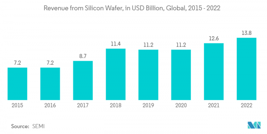
- The rise in the expansion of the wafer production plants will create an opportunity for the local and international wafer inspection players to develop new products according to the customer's requirements. For instance, according to SEMI, in 2022, the silicon wafer area shipments worldwide amounted to 14.71 billion square inches, which increased from 14.16 billion square inches in 2021. Silicon wafers are a vital building material for semiconductors, which indicates the usage of high-performance semiconductors in connected devices and driving the market. Further, in 2022, the total revenue from silicon wafers worldwide amounted to USD 13.8 billion, which increased from USD 12.6 billion, further indicating the market's growth.
Asia-Pacific to Dominate the Market
- The Asia-Pacific is one of the prominent regions for the semiconductor industry concerning manufacturing and consumption. According to SIA, Asia-Pacific is the largest regional semiconductor market, and China accounts for the most significant share in the region.
- Many regional companies are entering collaborations and partnerships in the semiconductor metrology/inspection equipment market. For instance, Shenzhen JT Automation Equipment, a chip production tool manufacturer in China, announced a legally binding five-year (2021-2025) memorandum of understanding with Huawei's HiSilicon Technologies business, China's largest chip developer. Both firms aim to extend their partnership for the development of semiconductor packaging tools, creating a self-sufficient and regulated industry.
- Asia-Pacific has been a growing market for semiconductor equipment over the last few years. For instance, according to SEMI, in 2022, China remained the leading spender on semiconductor equipment with USD 28.3 billion in billings. However, trade issues between the United States and China have presented uncertainty in the semiconductor metrology and inspection equipment market. Domestic semiconductor companies have been spending significantly to maintain their current market position by increasing their capacity and transitioning between technology nodes and wafer sizes. In the future, the demand is expected to be witnessed from the foundry in the region.
- The regional government's initiatives to develop the local semiconductor industry also creates a favorable outlook for the growth of the studied market. For instance, China's State Council's "National Integrated Circuit Industry Development Guidelines" aims to make the country a global leader in all the segments of the semiconductor industry by 2030. Additionally, the Made in China 2025 initiative maintains achieving knowledge concerning advanced semiconductor manufacturing as a vital component of China's future economy. It is highly focused on building the strategy for a strong manufacturing nationwide.
- The initiative is also expected to encourage local and foreign companies to invest in various segments of semiconductor manufacturing including integrated circuits. The initiative prompts the government bodies to boost research and development activities so that China can rely on its own companies for core technologies rather than overseas ones. This is set to propel innovation in the semiconductor manufacturing industry.
Semiconductor Metrology & Inspection Equipment Industry Overview
The semiconductor metrology and inspection equipment market comprises prominent players such as Applied Materials Inc., Nikon Metrology NV, and KLA Corporation. These firms have continuously expanded their operation scales by focusing on market expansions and acquisitions. Acquisition activities effectively set the ball rolling regarding the overall market's growth in the market studied. Large companies have also been expending significant resources on R&D operations to protect their market position and drive innovation in the studied market shortly. Overall, the degree of competition remains high, primarily driven by the strong presence of prominent players involved in the market studied.
- July 2023: Applied Materials Inc. introduced materials, technologies, and systems that help chipmakers integrate chiplets into advanced 2.5D and 3D packages using hybrid bonding and through-silicon vias (TSVs). The new solutions will extend the company's industry-leading breadth of technologies for heterogeneous integration (HI). The company is the largest supplier of technologies for HI with optimized chipmaking systems spanning etch, physical and chemical vapor deposition (PVD), electroplating, chemical mechanical polishing (CMP), annealing, and surface treatments.
- May 2023: KLA Corporation announced a strategic partnership with imec to develop the talent base and infrastructure to accelerate the advanced semiconductor applications for autonomous mobility, electrification and move the automotive industry forward. Through this partnership, both partners plan to bring relevant expertise to identify and manage programs for automotive industry, as well as talent development and recruitment.
Additional Benefits:
- The market estimate (ME) sheet in Excel format
- 3 months of analyst support
TABLE OF CONTENTS
1 INTRODUCTION
- 1.1 Study Assumptions and Market Definition
- 1.2 Scope of the Study
2 RESEARCH METHODOLOGY
3 EXECUTIVE SUMMARY
4 MARKET INSIGHTS
- 4.1 Market Overview
- 4.2 Industry Attractiveness - Porter's Five Forces Analysis
- 4.2.1 Bargaining Power of Suppliers
- 4.2.2 Bargaining Power of Buyers
- 4.2.3 Threat of New Entrants
- 4.2.4 Threat of Substitutes
- 4.2.5 Degree of Competition
- 4.3 An Assessment of the Impact of Key Macro Trends
5 MARKET DYNAMICS
- 5.1 Market Drivers
- 5.1.1 Increasing Demand for High-performance, Low-cost Semiconductors
- 5.1.2 Increasing Demand for Semiconductor Wafers in Consumer Electronics
- 5.2 Market Restraints
- 5.2.1 High Setup Cost and Lack of Expertise in Handling Metrology Systems Efficiently
- 5.2.2 High Raw Material and Fabrication Costs
6 MARKET SEGMENTATION
- 6.1 By Type
- 6.1.1 Lithography Metrology
- 6.1.1.1 Overlay
- 6.1.1.2 Dimension Equipment
- 6.1.1.3 Mask Inspection and Metrology
- 6.1.2 Wafer Inspection
- 6.1.3 Thin Film Metrology
- 6.1.4 Other Process Control Systems
- 6.1.1 Lithography Metrology
- 6.2 By Geography
- 6.2.1 North America
- 6.2.2 Europe
- 6.2.3 Asia-Pacific
- 6.2.4 Rest of the World
7 COMPETITIVE LANDSCAPE
- 7.1 Company Profiles
- 7.1.1 KLA Corporation
- 7.1.2 Applied Materials Inc.
- 7.1.3 Onto Innovation Inc.
- 7.1.4 Thermo Fisher Scientific Inc.
- 7.1.5 Hitachi Hi-Technologies Corporation (Hitachi Limited)
- 7.1.6 Nova Measuring Instruments Ltd
- 7.1.7 ASML Holding NV
- 7.1.8 Lasertec CorporatioN
- 7.1.9 JEOL Ltd
- 7.1.10 Nikon Metrology NV (Nikon Group)
- 7.1.11 Camtek Limited
8 INVESTMENT ANALYSIS
9 FUTURE OF THE MARKET
 2024 年半導體計量與檢測全球市場報告
 半導體計量和檢測市場報告:2030 年趨勢、預測和競爭分析
 半導體測量·檢驗的全球市場 - 主要趨勢與機會(~2029年)
 半導體計量設備市場 - 2023-2031年全球行業分析、規模、佔有率、成長、趨勢和預測
 不穩定(瞬態)分析軟件全球市場規模研究和預測:按組件、部署模型、公司規模、最終用戶、地區劃分,2022-2029 年
 全球半導體計量和檢測設備市場 - 按類型、組織規模和地區劃分的市場規模、細分市場、前景和收入預測(2022-2028 年)
 半導體計量與檢測市場:按類型、技術、組織規模分類:2021-2031 年全球機遇分析和行業預測
 半導體測量·檢驗的全球市場預測(到2028年):COVID-19影響,類型,技術,各組織規模的分析