


|
市場調查報告書
商品編碼
1868994
物聯網半導體設計與製造生態系統市場:2025-2030IoT Semiconductor Design and Manufacturing Ecosystem Market Report 2025-2030 |
|||||||
本報告詳細分析了物聯網半導體設計與製造生態系統,包括市場規模、關鍵趨勢和市場佔有率,涵蓋電子設計自動化 (EDA) 和半導體智慧財產權 (IP) 市場以及代工(製造)市場。
範例預覽
全球物聯網設備的安裝數量持續成長,每個設備內部的半導體密度也隨之提高。這項需求成長是由複雜的物聯網半導體價值鏈驅動的,負責底層晶片的設計和製造。
本報告對物聯網半導體價值鏈進行了系統分析,重點在於設計和製造生態系統。其主要目標是透過定義、評估和分析價值鏈的三個基礎(EDA、半導體IP和代工廠),幫助讀者更好地理解這一領域。
報告摘要
報告概述
- 148頁報告: 全面分析物聯網半導體價值鏈,重點在於關於設計、IP 和製造生態系統。
- 三大技術深度分析: 對 EDA、半導體 IP 和代工廠的詳細分析。
- 五大半導體宏觀趨勢: 分析影響物聯網半導體價值鏈的宏觀趨勢,包括人工智慧、國家安全和地緣政治。
- 供應商市場佔有率分析: 區隔 EDA、IP 和代工廠領域的競爭格局。
- 市場規模與預測: 分析物聯網 EDA、IP 與代工廠市場,預測至 2030 年。
主要分析領域
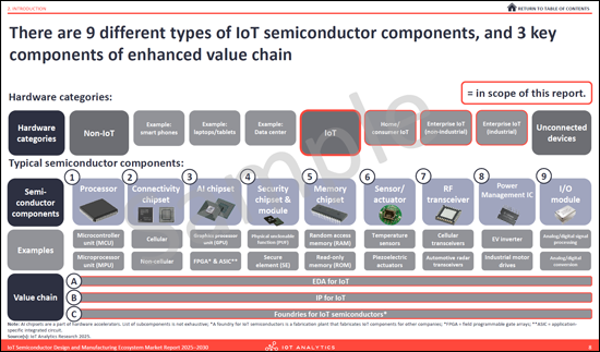
- 物聯網半導體概述: 定義了九類半導體組件,並描述了本報告分析的物聯網半導體價值鏈的三大主要部分。
- 物聯網半導體市場概況: 提供物聯網半導體組件的市場支出狀況,以及設計與製造價值鏈的市場支出分析。此外,也概述了影響市場動態的五大跨產業趨勢。
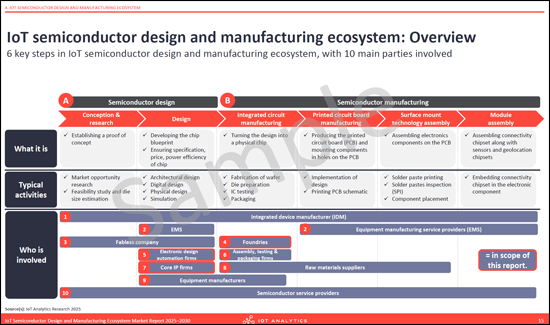
- 物聯網半導體價值鏈概覽: 描繪了設計和製造生態系統中的六個關鍵步驟和十個主要利害關係人群體。探討了四大關鍵技術趨勢,包括依區隔市場和地區劃分的市場支出。
- 物聯網EDA深度分析: 考察晶片設計和驗證流程,從系統規格到製造和測試。提供區域支出分析、市場佔有率、主要供應商概況以及四大新興趨勢。
- 物聯網IP深度分析: 涵蓋四大主要半導體IP類別(處理器、介面、記憶體和安全)及其區隔市場。包括區域市場規模、競爭格局評估和主要供應商概況。
- 物聯網晶圓代工深度解析:概述半導體製造流程(晶圓製備、製造、組裝、測試和封裝的演變)。內容包括區域支出、市場佔有率分析以及領先晶圓代工廠的概況。
公司列表:
|
|
|
目錄
第一章:摘要整理
第二章:引言
- 章節概述
- 出發點:物聯網設備的數量持續成長,預計到2030年將達到390億。
- 每個設備內部的半導體密度也不斷增加。
- 物聯網半導體元件共有九種類型,其中增強型價值鏈包含三種關鍵元件。
- 定義:半導體和物聯網半導體
- 定義:處理器
- 定義:連接晶片組
- 定義:人工智慧晶片組
- 定義:安全晶片組
- 定義:其他
第三章 概覽:物聯網半導體市場
- 章節概述
- 概述:物聯網半導體市場分為兩部分
- 第一部分:物聯網半導體元件 - 依類型劃分的支出
- 第二部分:物聯網半導體設計與製造生態系統 - 依區隔市場劃分的支出
- 物聯網半導體整體競爭格局
- 物聯網區隔市場對多家半導體公司的重要性
- 影響物聯網半導體的五大趨勢
- 近期發表的新半導體產品晶圓廠
- 研究方法:物聯網相關業務概況 - 台積電
物聯網半導體設計與製造生態系:概論
- 章節概述
- 物聯網半導體設計與製造生態系:概述
- 物聯網半導體設計與製造生態系:定義
- 物聯網半導體設計與製造市場支出 - 概述
- 物聯網半導體設計與製造分析師評論
- 物聯網半導體設計與製造市場支出 - 依區隔市場劃分
- 物聯網半導體設計與製造市場支出 - 依地區劃分
- 競爭格局:物聯網半導體設計與製造生態系統中的主要供應商
- 趨勢
第五章:物聯網EDA
- 章節概述
- 物聯網半導體設計:概述
- 晶片設計與驗證
- 印刷電路板設計:製程概述
- 異質整合:概述
- 全球物聯網EDA支出概況:2020-2030
- 分析師對物聯網EDA的評論
- 全球物聯網EDA支出預測 - 依地區劃分:2020-2030
- 競爭格局:物聯網EDA市場的主要供應商
- 物聯網EDA競爭格局
- 主要公司簡介:Cadence
- 主要公司簡介:Synopsys
- 趨勢
第六章 物聯網IP
- 章節概述
- 物聯網IP
- 全球物聯網IP支出概況:2020-2030
- 分析師對物聯網IP的評論
- 全球物聯網IP支出(依地區劃分): 2020-2030
- 競爭格局:物聯網市場領先的IP供應商
- 物聯網IP競爭格局
- 主要公司簡介:Arm
第七章:物聯網晶圓代工廠
- 章節概述
- 物聯網晶片組半導體製造
- 全球物聯網支出概況:晶圓代工廠:2020-2030
- 分析師對物聯網晶圓代工廠的評論
- 全球物聯網支出:晶圓代工廠 - 依地區劃分:2020-2030
- 競爭格局:領先的物聯網晶圓代工廠
- 物聯網晶圓代工廠競爭格局
- 主要公司簡介:台積電
第八章:研究方法與市場定義
第九章:物聯網分析概論
A 148-page report detailing the IoT semiconductor design and manufacturing ecosystem, covering EDA and IP markets as well as foundries, with market sizing, key trends, and market shares.
Sample preview
The global installed base of connected IoT devices continues to expand, driving a corresponding increase in semiconductor density within each device. This growing demand is supported by a complex IoT semiconductor value chain responsible for designing and manufacturing the underlying chips.
This report provides a structured IoT semiconductor value chain analysis, focusing on the design and manufacturing ecosystem. Its primary objective is to help readers understand this landscape by defining, sizing, and analyzing the three foundational pillars of the value chain: Electronic Design Automation (EDA), Semiconductor Intellectual Property (IP), and Foundries.
The findings are based on extensive primary research, including interviews with semiconductor experts from leading vendors and end-user organizations across the IoT semiconductor value chain, complemented by secondary research and insights gathered from major industry trade fairs.
Sample preview
Report at a glance
- 148-page report: A comprehensive analysis of the IoT semiconductor value chain, focusing on the design, IP, and manufacturing ecosystem.
- 3 technology deep dives: In-depth analyses of Electronic Design Automation (EDA), Semiconductor Intellectual Property (IP), and Foundries for IoT.
- 5 overarching semiconductor trends: Examination of macro trends (e.g., AI, security, geopolitics) impacting the IoT semiconductor value chain.
- Vendor market share analysis: A breakdown of the competitive landscape for each of the three ecosystem segments (EDA, IP, and Foundries).
- Market sizing and forecast: Market analysis for the EDA, IP, and Foundry for IoT markets, with forecasts to 2030.
Key areas of analysis
- Introduction to IoT semiconductors: Defines nine categories of semiconductor components and explains the three key segments of the IoT semiconductor value chain analyzed in this report.
- Big picture-The IoT semiconductor market: Provides market spending analysis for both IoT semiconductor components and the design/manufacturing segments of the IoT semiconductor value chain. Also outlines five cross-industry trends influencing market dynamics.
- Overview of the IoT semiconductor value chain: Maps the six critical steps and ten primary stakeholder groups within the design and manufacturing ecosystem. Includes market spending by segment and region and explores four major technical trends.
- EDA for IoT deep dive: Examines the chip design and verification process from system specification to fabrication and testing. Provides regional spending analysis, market share insights, key vendor profiles, and four emerging trends.
- IP for IoT deep dive: Covers the four main types of semiconductor IP (Processor, Interface, Memory, and Security) and their sub-segments. Includes regional market sizing, competitive landscape assessment, and a leading vendor profile.
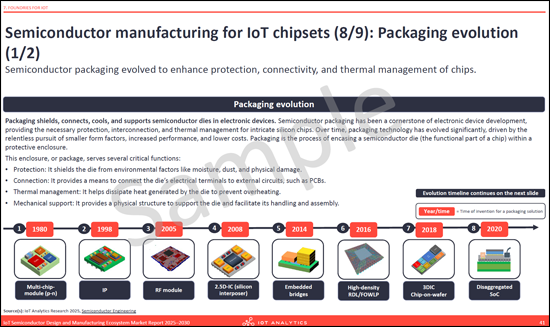
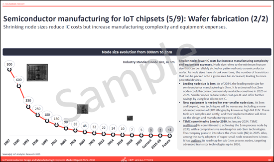
- Foundries for IoT deep dive: Outlines the semiconductor manufacturing process, including wafer preparation, fabrication, assembly, testing, and packaging evolution. Analyzes regional spending, market shares, and includes a leading foundry profile.
A data-driven foundation for key business functions
- Strategy and corporate development: Inform strategic planning with market sizing, 2030 forecasts, and analysis of macro trends impacting the IoT semiconductor value chain, such as geopolitical shifts and supply chain diversification.
- Product management and marketing: Guide product and technology roadmaps using detailed analyses of emerging technology trends and competitive dynamics across the EDA, IP, and foundry segments of the IoT semiconductor value chain.
- R&D and engineering leadership: Direct technical priorities with insights into EDA workflows, IP block architectures, and advanced packaging innovations, along with trends such as security-by-design and cloud-based design platforms.
- Market intelligence and competitive analysis: Benchmark market position within the IoT semiconductor value chain using granular market share data and vendor profiles for the EDA, IP, and foundry segments.
Key concepts defined
- IoT semiconductor value chain: The ecosystem of companies and processes involved in chip creation, defined in this report by six key stages: conception & research, design, integrated circuit manufacturing, printed circuit board manufacturing, surface mount technology assembly, and module assembly.
- Electronic design automation (EDA) for IoT: A key segment of the IoT semiconductor value chain providing software and tools used to design silicon or modules for IoT endpoints or gateways. Includes RTL design, simulation, verification, synthesis, analog/mixed-signal, DFT, advanced packaging, and PCB tools.
- Semiconductor intellectual property (IP) for IoT: A foundational segment of the IoT semiconductor value chain comprising licenses and royalties derived from integrating reusable IP blocks (IP cores) into silicon for IoT devices.
- Foundries for IoT: The manufacturing segment of the IoT semiconductor value chain that provides wafer fabrication and advanced packaging services for chips designed by fabless semiconductor companies.
- Chiplet: A small, specialized IC designed to interconnect with other chiplets or larger ICs. This modular structure enables integration of multiple chips using different process nodes within a single package.
- Heterogeneous integration: A manufacturing approach that combines multiple, separately manufactured components (chips, chiplets, etc.) into a single package, often using different materials and processes.
Questions answered:
- Which stakeholders are involved across EDA, IP, and foundry stages of the value chain?
- Which technologies are critical across EDA, IP, and foundries in enabling IoT semiconductor development?
- What is the current and projected market size of EDA, IP, and foundry for IoT markets?
- What is the market share of leading vendors across these three segments?
- What trends are shaping the future of the IoT semiconductor design and manufacturing ecosystem?
Companies mentioned:
A selection of companies mentioned in the report.
|
|
|
Table of Contents
1. Executive summary
2. Introduction
- Chapter overview: Introduction
- Starting point: The number of loT connected devices continues to grow - Expected to reach 39 billion by 2030
- The semiconductor density within each device also continues to increase
- There are 9 different types of IoT semiconductor components, and 3 key components of enhanced value chain.
- Definitions (1/6): Semiconductors & IoT semiconductors
- Definitions (2/6): Processors
- Definitions (3/6): Connectivity chipsets
- Definitions (4/6): AI chipsets
- Definitions (5/6): Security chipsets
- Definitions (6/6): Other key components
3. Big picture: The IoT semiconductor market
- Chapter overview: Big picture: The IoT semiconductor market
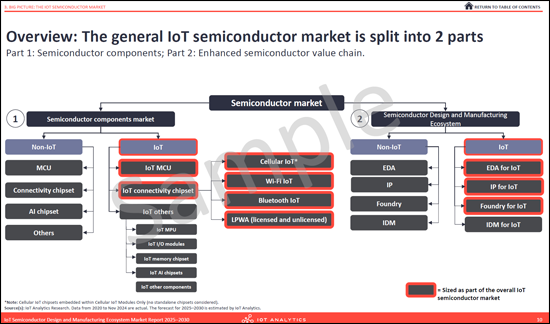
- Overview: The general IoT semiconductor market is split into 2 parts
- Part 1: IoT semiconductor components - Spending by type
- Part 2: IoT semiconductor design and manufacturing ecosystem - Spending by segment
- Overall IoT semiconductor competitive landscape
- Importance of IoT as a segment within several chip companies
- 5 overarching trends impacting IoT semiconductors
- Overarching trend 1
- Overarching trend 2
- Overarching trend 3
- Overarching trend 4
- Overarching trend 5
- Recent announcements for new semiconductor plants
- Methodology: Mapping IoT-related business - TSMC
IoT semiconductor design and manufacturing ecosystem: Overview
- Chapter overview: IoT semiconductor design and manufacturing ecosystem: Overview
- IoT semiconductor design and manufacturing ecosystem: Overview
- IoT semiconductor design and manufacturing ecosystem: Definitions
- IoT semiconductor design and manufacturing market spending - Overview
- Analyst commentary on the IoT semiconductor design and manufacturing
- IoT semiconductor design and manufacturing market spending - By segment
- IoT semiconductor design and manufacturing market spending - By region
- Competitive landscape: Key vendors in IoT semiconductor design and manufacturing ecosystem
- Trend 1
- Trend 2
- Trend 3
- Trend 4
5. EDA for IoT
- Chapter overview: EDA for IoT
- IoT semiconductor design: Overview
- Chip design and verification
- Printed circuit board design: Process overview
- Heterogeneous integration: Overview
- Global EDA for IoT spending 2020-2030 - Overview
- Analyst commentary on the EDA for IoT
- Global EDA for IoT spending 2020-2030 - By region
- Competitive landscape: Key vendors in EDA for IoT market
- EDA for IoT competitive landscape
- Key company profile: Cadence
- Key company profile: Synopsys
- Trend 1
- Trend 2
- Trend 3
- Trend 4
6. IP for IoT
- Chapter overview: IP for IoT
- IP for IoT
- Global IP for IoT spending 2020-2030 - Overview
- Analyst commentary on the IP for IoT
- Global IP for IoT spending 2020-2030 - By region
- Competitive landscape: Key vendors in IP for IoT market
- IP for IoT competitive landscape
- Key company profile: Arm
7. Foundries for IoT
- Chapter overview: Foundries for IoT
- Semiconductor manufacturing for IoT chipsets
- Global Foundry for IoT spending 2020-2030 - Overview
- Analyst commentary on the Foundries for IoT
- Global Foundry for IoT spending 2020-2030 - By region
- Competitive landscape: Key foundries for IoT
- Foundries for IoT competitive landscape
- Key company profile: TSMC
8. Methodology & market definitions
- Key market definitions
- Country mappings to regions
- Research Methodology
9. About IoT Analytics
 半導體元件清洗市場:依清潔劑、清洗設備、產業、清洗製程、材料類型、國家及地區分類-全球產業分析、市場規模、市場佔有率及2026年至2033年預測半導體及電路製造市場:依產品類型、應用、組件、晶圓尺寸、材料、國家及地區分類-全球產業分析、市場規模、市場佔有率及2026年至2033年預測
 全球半導體晶片生態系統市場:機會與策略展望(至2035年)
 半導體產業:市場佔有率分析、產業趨勢與統計、成長預測(2026-2031)
 2026 年至 2035 年電氣金屬管材的市場機會、成長要素、產業趨勢分析與預測。半導體及相關裝置市場:全球產業分析、市場規模、市場佔有率及預測(2026-2033 年),依半導體類型、裝置類型、材料類型、技術、應用、國家及地區分類半導體智慧電網市場:按組件、功能、應用、最終用戶、國家和地區分類-行業分析、市場規模、市場佔有率和預測(2026-2033 年)半導體物流:市場佔有率分析、產業趨勢與統計、成長預測(2026-2031)
 2026-2030年全球半導體市場
 用於替代能源技術的半導體:機會和市場