

 |
市場調查報告書
商品編碼
2071362
半導體工廠建設市場機會、成長要素、產業趨勢分析及2026-2035年預測。Semiconductor Plant Construction Market Opportunity, Growth Drivers, Industry Trend Analysis, and Forecast 2026 - 2035 |
||||||

全球半導體工廠建設市場預計到 2025 年將達到 472 億美元,到 2035 年將以 4.1% 的複合年成長率成長,達到 850 億美元。
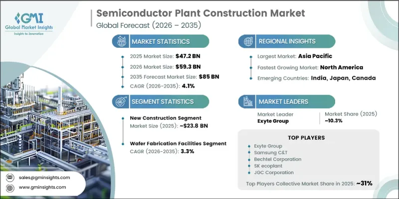
這一成長的驅動力來自快速的數位轉型、下一代技術中半導體整合度的提高,以及旨在增強供應鏈韌性的大規模投資。製造商正積極透過新建工廠和改造現有晶圓廠來擴大產能,以滿足全球對高性能晶片日益成長的需求。政府主導的措施也發揮著至關重要的作用,透過政策支持、獎勵和資金計劃,加強國內半導體生態系統,並透過生產基地的集中化來降低對海外的依賴。晶圓製造設施仍然是該行業的核心,在實現先進積體電路所需的精密製造流程方面發揮著至關重要的作用。製程節點的持續創新,以及節能高效生產環境的採用,進一步推動了全球半導體生態系統的建設活動。
| 市場範圍 | |
|---|---|
| 開始年份 | 2025 |
| 預測期 | 2026-2035 |
| 上市時的市場規模 | 472億美元 |
| 預測金額 | 850億美元 |
| 複合年成長率 | 4.1% |
預計到2025年,這一新興細分市場規模將達到238億美元,並在2035年之前保持2.6%的複合年成長率。全球半導體製造能力的擴張和對先進生產基礎設施需求的不斷成長,並持續推動著這個細分市場的發展。來自公共和私人相關人員者的積極投資,支持旨在增強供應鏈穩定性並滿足多個終端用戶行業日益成長的需求的待開發區製造項目。
預計到2025年,晶圓製造設施細分市場將佔據77.7%的市場佔有率,並在2035年之前以3.3%的複合年成長率成長。這個細分市場之所以能夠推動市場成長,是因為它在半導體製造中扮演著至關重要的角色,而半導體製造則涉及光刻、摻雜、蝕刻和沈積等高度複雜的製程。人工智慧、電動車、通訊和高效能運算等領域對先進晶圓的需求不斷成長,推動了晶圓製造工廠建設的持續投資。
中國半導體工廠建設市場預計到2025年將達到84億美元,並在2035年之前以4.2%的複合年成長率成長。這一市場擴張得益於一項旨在提升國內半導體產能、減少對進口晶片依賴的國家戰略。在家用電子電器、通訊和工業應用等需求的驅動下,中國大規模投資於成熟和先進製程技術的製造基礎建設。
目錄
第1章:調查方法和範圍
第2章執行摘要
第3章 行業洞察
- 產業生態系分析
- 供應商情況
- 利潤率
- 每個階段增加的價值
- 影響價值鏈的因素
- 影響產業的因素
- 促進因素
- 人工智慧、5G、汽車和資料中心等因素推動半導體需求快速成長。
- 政府激勵措施和國家半導體戰略計劃
- 推動製造業回流和供應鏈多元化的舉措
- 潛在風險和挑戰
- 極高的資本投入和漫長的建設週期
- 潔淨室和精密環境中的複雜技術要求
- 機會
- 擴大亞太和北美地區的半導體製造能力
- 人工智慧驅動的施工規劃數位雙胞胎技術的應用
- 促進因素
- 成長潛力分析
- 未來市場趨勢
- 技術與創新展望
- 最新科技趨勢
- 新興技術
- 監理情勢
- 標準和合規要求
- 區域監理框架
- 認證標準
- 波特的分析
- PESTLE分析
- 價格分析
- 對過去價格趨勢的分析
- 依專案規模(小規模/中型/大型晶圓廠)制定定價策略
- 人工智慧和生成式人工智慧對市場的影響
- 利用人工智慧改造現有建築模型
- 生成式人工智慧的應用案例與實施藍圖
- 晶圓廠佈局的衍生設計
- 人工智慧驅動的調度和資源最佳化
- 施工機械的預測性維護
- 風險、限制和監管考量
- 生產能力和生產情況
- 全球晶圓廠運作按地區和技術節點分類
- 運轉率和擴張計劃
第4章 競爭情勢
- 介紹
- 企業市佔率分析
- 按地區
- 企業矩陣分析
- 主要市場公司的競爭分析
- 競爭定位矩陣
- 主要進展
- 併購
- 夥伴關係和聯盟
- 新產品發布
- 業務拓展計劃
第5章 市場估價與預測:依建築類型分類,2022-2035年
- 新建工程
- 擴張
- 維修
第6章 市場估價與預測:依設施類型分類,2022-2035年
- 晶圓製造廠
- 組裝和測試設施
- 研究與開發設施
第7章 市場估計與預測:依設備類型分類,2022-2035年
- 光刻
- 成膜
- 蝕刻
- 化學機械拋光(CMP)
- 打掃
- 其他
第8章 市場估算與預測:依專案實施模式分類,2022-2035年
- EPC/承包
- 設計建造方法
- 施工管理
- 合資/聯合體
第9章 市場估計與預測:依地區分類,2022-2035年
- 北美洲
- 美國
- 加拿大
- 歐洲
- 德國
- 英國
- 法國
- 義大利
- 西班牙
- 亞太地區
- 中國
- 印度
- 日本
- 韓國
- 澳洲
- 拉丁美洲
- 巴西
- 墨西哥
- 阿根廷
- 中東和非洲
- 沙烏地阿拉伯
- UAE
- 南非
第10章:公司簡介
- 世界頂尖公司
- Bechtel Corporation
- Exyte
- Fluor Corporation
- Jacobs Engineering Group
- Samsung C&T Corporation
- SK ecoplant
- JGC Corporation
- 該地區的領先企業
- DPR Construction
- Gilbane Building Company
- Tata Projects Limited
- Hoffman Construction
- Kajima Corporation
- Obayashi Corporation
- Mortenson
- 新興企業和專業公司
- PCL Construction
- Hensel Phelps
- Skanska
- Austin Industries
- Sundt Construction
- Kiewit Corporation
- 麥卡錫建築公司
The Global Semiconductor Plant Construction Market was valued at USD 47.2 billion in 2025 and is estimated to grow at a CAGR of 4.1% to reach USD 85 billion by 2035.
Growth is fueled by rapid digital transformation, increasing semiconductor intensity in next-generation technologies, and large-scale investments aimed at strengthening supply chain resilience. Manufacturers are aggressively expanding production capacity through both new facility development and modernization of existing fabs to meet escalating global demand for high-performance chips. Government-led initiatives are also playing a crucial role, with policy support, incentives, and funding programs designed to enhance domestic semiconductor ecosystems and reduce reliance on concentrated production hubs. Wafer fabrication facilities remain central to the industry, given their role in enabling precision-driven manufacturing processes required for advanced integrated circuits. Continuous innovation in process nodes, coupled with increasing adoption of energy-efficient and high-yield production environments, is further driving construction activity across global semiconductor ecosystems.
| Market Scope | |
|---|---|
| Start Year | 2025 |
| Forecast Year | 2026-2035 |
| Start Value | $47.2 Billion |
| Forecast Value | $85 Billion |
| CAGR | 4.1% |
The new construction segment accounted for USD 23.8 billion in 2025 and is projected to grow at a CAGR of 2.6% through 2035. This segment continues to dominate due to the expansion of global chip manufacturing capacity and the rising need for advanced production infrastructure. Strong investments from both public and private stakeholders are supporting greenfield fabrication projects aimed at enhancing supply chain stability and meeting growing demand from multiple end-use industries.
The wafer fabrication facilities segment held 77.7% share in 2025 and is expected to grow at a CAGR of 3.3% through 2035. This segment leads the market due to its essential role in semiconductor manufacturing, where wafers undergo highly complex processes such as lithography, doping, etching, and deposition. Increasing demand for advanced chips used in artificial intelligence, electric mobility, telecommunications, and high-performance computing is driving continuous investment in wafer fab construction.
China Semiconductor Plant Construction Market reached USD 8.4 billion in 2025 and is projected to grow at a CAGR of 4.2% through 2035. Market expansion is strongly supported by national strategies focused on strengthening domestic semiconductor production capabilities and reducing dependence on imported chips. Large-scale investments are being directed toward expanding fabrication infrastructure across both mature and advanced process technologies, driven by demand from consumer electronics, telecommunications, and industrial applications.
Key companies operating in the global semiconductor plant construction market include Bechtel Corporation, Exyte, Fluor Corporation, Jacobs Engineering Group, SK ecoplant, Samsung C&T Corporation, JGC Corporation, DPR Construction, Gilbane Building Company, Mortenson, Hoffman Construction, Kajima Corporation, Obayashi Corporation, Tata Projects Limited, Skanska, PCL Construction, Hensel Phelps, Austin Industries, Sundt Construction, Kiewit Corporation, and McCarthy Building Companies. Market participants are strengthening their competitive positioning through large-scale EPC capabilities and advanced cleanroom construction expertise tailored for semiconductor fabrication environments. Companies are investing in high-precision engineering solutions to support next-generation process nodes and ultra-clean manufacturing requirements. Strategic collaborations with semiconductor manufacturers and technology providers are enabling long-term project pipelines and improved execution efficiency. Firms are also focusing on modular construction techniques and digital project management tools to reduce build times and improve cost efficiency. Expansion into new geographic markets supported by government-backed semiconductor programs is further enhancing growth opportunities.
Table of Contents
Chapter 1 Methodology & Scope
- 1.1 Market scope and definition
- 1.2 Research design
- 1.2.1 Research approach
- 1.2.2 Data collection methods
- 1.3 Data mining sources
- 1.3.1 Global
- 1.3.2 Regional/Country
- 1.4 Base estimates and calculations
- 1.4.1 Base year calculation
- 1.4.2 Key trends for market estimation
- 1.5 Primary research and validation
- 1.5.1 Primary sources
- 1.6 Forecast model
- 1.7 Research assumptions and limitations
Chapter 2 Executive Summary
- 2.1 Industry 360° synopsis
- 2.2 Key market trends
- 2.2.1 Regional
- 2.2.2 Construction Type
- 2.2.3 Facility
- 2.2.4 Equipment
- 2.2.5 Project Delivery Model
Chapter 3 Industry Insights
- 3.1 Industry ecosystem analysis
- 3.1.1 Supplier landscape
- 3.1.2 Profit margin
- 3.1.3 Value addition at each stage
- 3.1.4 Factor affecting the value chain
- 3.2 Industry impact forces
- 3.2.1 Growth drivers
- 3.2.1.1 Rapid expansion of semiconductor demand from AI, 5G, automotive, and data centers
- 3.2.1.2 Government incentives and strategic national semiconductor programs
- 3.2.1.3 Reshoring and supply chain diversification initiatives
- 3.2.2 Pitfalls & Challenges
- 3.2.2.1 Extremely high capital investment and long construction timelines
- 3.2.2.2 Complex engineering requirements for cleanrooms and precision environments
- 3.2.3 Opportunities
- 3.2.3.1 Expansion of semiconductor manufacturing capacity in Asia Pacific and North America
- 3.2.3.2 Adoption of AI-driven construction planning and digital twin technologies
- 3.2.1 Growth drivers
- 3.3 Growth potential analysis
- 3.4 Future market trends
- 3.5 Technology and innovation landscape
- 3.5.1 Current technological trends
- 3.5.2 Emerging technologies
- 3.6 Regulatory landscape
- 3.6.1 Standards and compliance requirements
- 3.6.2 Regional regulatory frameworks
- 3.6.3 Certification standards
- 3.7 Porter's analysis
- 3.8 PESTEL analysis
- 3.9 Pricing analysis (solution core) (driven by primary research)
- 3.9.1 Historical price trend analysis (driven by primary research)
- 3.9.2 Pricing strategy by project scale (small/medium/large-scale fabs) (driven by primary research)
- 3.10 Impact of AI and generative AI on the market
- 3.10.1 AI-driven disruption of existing construction models
- 3.10.2 GenAI use cases and adoption roadmap
- 3.10.3 Generative design for fab layouts
- 3.10.4 AI-powered scheduling and resource optimization
- 3.10.5 Predictive maintenance for construction equipment
- 3.10.6 Risks, limitations and regulatory considerations
- 3.11 Capacity and production landscape (driven by primary research)
- 3.11.1 Installed global fab capacity by region and technology node (driven by primary research)
- 3.11.2 Capacity utilization rates and expansion pipelines (driven by primary research)
Chapter 4 Competitive Landscape, 2025
- 4.1 Introduction
- 4.2 Company market share analysis
- 4.2.1 By Region
- 4.2.1.1 North America
- 4.2.1.2 Europe
- 4.2.1.3 Asia Pacific
- 4.2.1.4 Latin America
- 4.2.1.5 Middle East & Africa
- 4.2.1 By Region
- 4.3 Company matrix analysis
- 4.4 Competitive analysis of major market players
- 4.5 Competitive positioning matrix
- 4.6 Key developments
- 4.6.1 Mergers & acquisitions
- 4.6.2 Partnerships & collaborations
- 4.6.3 New product launches
- 4.6.4 Expansion plans
Chapter 5 Market Estimates & Forecast, By Construction Type, 2022 - 2035, (USD Billion) (Thousand Units)
- 5.1 Key trends
- 5.2 New construction
- 5.3 Expansion
- 5.4 Renovation
Chapter 6 Market Estimates & Forecast, By Facility, 2022 - 2035, (USD Billion) (Thousand Units)
- 6.1 Key trends
- 6.2 Wafer fabrication facilities
- 6.3 Assembly & test facilities
- 6.4 Research & development facilities
Chapter 7 Market Estimates & Forecast, By Equipment, 2022 - 2035, (USD Billion) (Thousand Units)
- 7.1 Key trends
- 7.2 Lithography
- 7.3 Deposition
- 7.4 Etching
- 7.5 Chemical mechanical planarization (CMP)
- 7.6 Cleaning
- 7.7 Others
Chapter 8 Market Estimates & Forecast, By Project Delivery Model, 2022 - 2035, (USD Billion) (Thousand Units)
- 8.1 Key trends
- 8.2 EPC/Turnkey
- 8.3 Design-Build
- 8.4 Construction Management
- 8.5 Joint Venture/Consortium
Chapter 9 Market Estimates & Forecast, By Region, 2022 - 2035, (USD Billion) (Thousand Units)
- 9.1 Key trends
- 9.2 North America
- 9.2.1 U.S.
- 9.2.2 Canada
- 9.3 Europe
- 9.3.1 Germany
- 9.3.2 UK
- 9.3.3 France
- 9.3.4 Italy
- 9.3.5 Spain
- 9.4 Asia Pacific
- 9.4.1 China
- 9.4.2 India
- 9.4.3 Japan
- 9.4.4 South Korea
- 9.4.5 Australia
- 9.5 Latin America
- 9.5.1 Brazil
- 9.5.2 Mexico
- 9.5.3 Argentina
- 9.6 MEA
- 9.6.1 Saudi Arabia
- 9.6.2 UAE
- 9.6.3 South Africa
Chapter 10 Company Profiles
- 10.1 Top Global Players
- 10.1.1 Bechtel Corporation
- 10.1.2 Exyte
- 10.1.3 Fluor Corporation
- 10.1.4 Jacobs Engineering Group
- 10.1.5 Samsung C&T Corporation
- 10.1.6 SK ecoplant
- 10.1.7 JGC Corporation
- 10.2 Regional Champions
- 10.2.1 DPR Construction
- 10.2.2 Gilbane Building Company
- 10.2.3 Tata Projects Limited
- 10.2.4 Hoffman Construction
- 10.2.5 Kajima Corporation
- 10.2.6 Obayashi Corporation
- 10.2.7 Mortenson
- 10.3 Emerging & Specialized Players
- 10.3.1 PCL Construction
- 10.3.2 Hensel Phelps
- 10.3.3 Skanska
- 10.3.4 Austin Industries
- 10.3.5 Sundt Construction
- 10.3.6 Kiewit Corporation
- 10.3.7 McCarthy Building Companies

 2026年全球半導體工廠建設市場報告
 全球半導體工廠計劃- 特別報告:Project Insight
 半導體工廠建設市場,按建設、按設施、按設備、按基礎設施、按國家和地區 - 2024-2032 年行業分析、市場規模、市場佔有率和預測