

 |
市場調查報告書
商品編碼
2038322
多束電子束微影術系統市場機會、成長要素、產業趨勢分析及2026-2035年預測。Multi-Beam E-Beam Lithography System Market Opportunity, Growth Drivers, Industry Trend Analysis, and Forecast 2026 - 2035 |
||||||

2025 年全球多束電子束微影術系統市場價值為 6.92 億美元,預計到 2035 年將以 7.5% 的複合年成長率成長至 14 億美元。
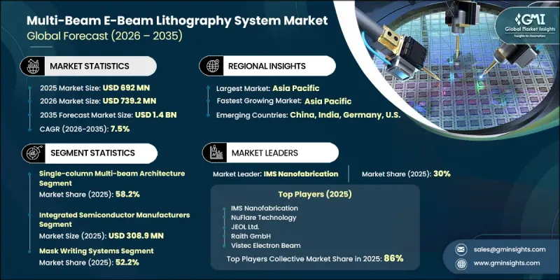
隨著半導體製造流程日益複雜,精度要求也日益嚴格,多束電子束微影術系統產業正穩步發展。向下一代晶片結構的轉型以及對高解析度圖形化日益成長的需求,推動了對先進掩模曝光解決方案的迫切需求。隨著人工智慧和資料中心運算環境中使用的半導體元件日趨複雜,對高精度微影術工具的需求也進一步成長。同時,向極紫外線(EUV)光掩模的轉變,也推動了能夠實現更高精度和吞吐量的系統的應用。全球製造設施的持續投資以及先進儲存技術的擴展,也為市場成長提供了支撐。總而言之,這些因素凸顯了多束系統在滿足不斷發展的半導體生產標準、同時確保更高的效率、可擴充性和性能方面所發揮的關鍵作用。
| 市場範圍 | |
|---|---|
| 開始年份 | 2025 |
| 預測期 | 2026-2035 |
| 上市時的市場規模 | 6.92億美元 |
| 預計金額 | 14億美元 |
| 複合年成長率 | 7.5% |
多束電子束微影術系統市場的成長與半導體製程節點向先進節點的轉變密切相關,這些節點對光罩曝光製程的處理速度、精度和吞吐量提出了更高的要求。隨著晶片製造商開發出更複雜的邏輯和記憶體元件,製造流程的複雜性不斷增加,從而導致對先進微影術解決方案的依賴性日益增強。專為資料密集型工作負載設計的處理器快速發展也推動了市場需求,因為這些應用需要複雜且高密度的電路圖案。這種日益成長的複雜性正在推動高解析度、高吞吐量系統的應用,以支援下一代半導體設計。
預計到2025年,單列多光束架構將佔據58.2%的市場佔有率,這主要得益於其在掩模曝光製程中始終如一的精度和穩定性能。與現有工作流程的兼容性以及在處理先進半導體應用方面的可靠性,也鞏固了其持續的主導地位。由於其解析度均勻且處理結果可靠,這些系統是高產量生產環境的首選。
預計到2025年,整合半導體製造商市場規模將達到3.089億美元。這一市場主導地位歸功於這些公司強大的生產能力以及對先進光掩模的持續需求,以支持尖端半導體技術的研發。隨著各公司致力於維持高精度、高產能和高圖案一致性,對先進微影術系統的需求依然強勁。
預計到2025年,北美多束電子束微影術系統市佔率將達到28.5%。隨著半導體製造商為滿足下一代生產需求而不斷採用包括EUV製程在內的先進微影術技術,該地區正經歷著穩定成長。該地區對高效能運算和先進半導體應用的需求日益成長,進一步加劇了對高精度、高複雜度圖形化解決方案的需求。這些趨勢持續提升了多束微影術系統在該地區半導體生態系的重要性。
目錄
第1章:調查方法和範圍
第2章執行摘要
第3章業界考察
- 生態系分析
- 供應商情況
- 利潤率
- 成本結構
- 每個階段增加的價值
- 影響價值鏈的因素
- 中斷
- 影響產業的因素
- 促進因素
- 對更先進的半導體製造的需求
- 高效能運算和人工智慧晶片的成長
- 擴大極紫外光微影和高數值孔徑極紫外光刻技術的應用
- 增加對全球新建半導體工廠的投資
- 更複雜的儲存技術需要精確的光罩圖案。
- 產業潛在風險與挑戰
- 多波束系統的高昂資本成本和複雜的運作特性
- 由於遮罩複雜性的增加,資料處理和吞吐量受到限制。
- 市場機遇
- 擴大無掩模微影術技術在先進封裝和專用元件的應用。
- 先進封裝技術的擴展推動了對高精度圖形化的需求。
- 促進因素
- 成長潛力分析
- 監理情勢
- 波特五力分析
- PESTEL 分析
- 科技與創新趨勢
- 當前技術趨勢
- 新興技術
- 價格趨勢
- 按地區
- 依產品
- 定價策略
- 新興經營模式
- 合規要求
- 專利和智慧財產權分析
第4章 競爭情勢
- 介紹
- 企業市佔率分析
- 按地區
- 市場集中度分析
- 主要公司的競爭標竿分析
- 財務績效比較
- 銷售量
- 利潤率
- 研究與發展(R&D)
- 產品系列比較
- 產品線寬度
- 科技
- 創新
- 區域擴張比較
- 全球擴張分析
- 服務網路覆蓋
- 按地區分類的市場滲透率
- 競爭定位矩陣
- 領導者
- 挑戰者
- 追蹤者
- 小眾玩家
- 戰略展望矩陣
- 財務績效比較
- 主要進展
- 併購
- 夥伴關係和聯盟
- 技術進步
- 業務拓展與投資策略
- 數位轉型計劃
- 新興/新創競爭對手的發展趨勢
第5章 市場估算與預測:依系統結構,2022-2035年
- 多柱式結構
- 高通量多柱系統(10 柱或更多)
- 中型多柱系統(5-10 柱)
- 低柱數多樑系統(少於5根柱)
- 單柱多樑結構
- 高光束數系統(10,000束或更多光束)
- 中等光束數系統(1,000 至 10,000 束光束)
第6章 市場估計與預測:依最終用戶產業分類,2022-2035年
- 半導體製造商
- 獨立光掩模製造商
- 學術和研究機構
第7章 市場估計與預測:依應用領域分類,2022-2035年
- 口罩暴露系統
- 直接晶圓寫入系統
第8章 市場估計與預測:依地區分類,2022-2035年
- 北美洲
- 美國
- 加拿大
- 歐洲
- 德國
- 英國
- 法國
- 西班牙
- 義大利
- 俄羅斯
- 亞太地區
- 中國
- 印度
- 日本
- 澳洲
- 韓國
- 拉丁美洲
- 巴西
- 墨西哥
- 阿根廷
- 中東和非洲
- 南非
- 沙烏地阿拉伯
- 阿拉伯聯合大公國
第9章:公司簡介
- 全球主要公司
- IMS Nanofabrication
- NuFlare Technology
- JEOL Ltd.
- Raith GmbH
- Vistec Electron Beam
- 按地區分類的主要公司
- 北美洲
- KLA Corporation
- Applied Materials
- 亞太地區
- Advantest Corporation
- Canon Inc.
- Hitachi High-Tech Corporation
- Elionix Inc.
- Toppan Photomasks
- 歐洲
- ASML Holding
- Mapper Lithography
- 北美洲
The Global Multi-Beam E-Beam Lithography System Market was valued at USD 692 million in 2025 and is estimated to grow at a CAGR of 7.5% to reach USD 1.4 billion by 2035.
The multi-beam e-beam lithography system industry is advancing steadily as semiconductor manufacturing moves toward increasingly complex designs and tighter precision requirements. Demand for advanced mask writing solutions is growing due to the transition to next-generation chip architectures and the rising need for high-resolution patterning. The increasing complexity of semiconductors used in artificial intelligence and data-centric computing environments is further intensifying the requirement for highly accurate lithography tools. At the same time, the shift toward extreme ultraviolet photomasks is driving adoption of systems capable of delivering superior precision and throughput. Ongoing investments in fabrication facilities worldwide and the expansion of advanced memory technologies are also supporting market growth. These factors collectively highlight the critical role of multi-beam systems in meeting evolving semiconductor production standards while ensuring efficiency, scalability, and performance improvements.
| Market Scope | |
|---|---|
| Start Year | 2025 |
| Forecast Year | 2026-2035 |
| Start Value | $692 Million |
| Forecast Value | $1.4 Billion |
| CAGR | 7.5% |
Growth in the multi-beam e-beam lithography system market is closely linked to the ongoing transition toward advanced semiconductor nodes that demand faster processing, higher accuracy, and improved throughput in mask writing operations. As chipmakers continue to develop more sophisticated logic and memory devices, manufacturing complexity continues to rise, increasing reliance on advanced lithography solutions. The rapid development of processors designed for data-intensive workloads is also contributing to demand, as these applications require intricate and densely packed circuit patterns. This growing complexity is driving the adoption of high-resolution, high-throughput systems capable of supporting next-generation semiconductor designs.
The single-column multi-beam architecture segment accounted for 58.2% share in 2025, supported by its ability to deliver consistent precision and stable performance in mask writing processes. Its compatibility with established workflows and its reliability in handling advanced semiconductor applications contribute to its continued leadership. These systems enable uniform resolution and dependable processing outcomes, making them a preferred choice for high-volume manufacturing environments.
The integrated semiconductor manufacturers segment reached USD 308.9 million in 2025. This dominance is attributed to the extensive production capabilities of these organizations and their continuous requirement for advanced photomasks to support cutting-edge semiconductor development. Their focus on maintaining high standards of accuracy, throughput, and pattern consistency ensures sustained demand for advanced lithography systems.
North America Multi-Beam E-Beam Lithography System Market accounted for 28.5% share in 2025. The region is experiencing steady expansion as semiconductor manufacturers increase adoption of advanced lithography technologies, including EUV-based processes, to support next-generation production requirements. Rising demand for high-performance computing and advanced semiconductor applications across regional markets is further strengthening the need for precise and high-complexity patterning solutions. These dynamics continue to reinforce the importance of multi-beam lithography systems in the region's semiconductor ecosystem.
Key companies operating in the Global Multi-Beam E-Beam Lithography System Market include IMS Nanofabrication, ASML Holding, NuFlare Technology, JEOL Ltd., Vistec Electron Beam GmbH, Raith GmbH, Advantest Corporation, Canon Inc., Hitachi High-Tech Corporation, Elionix Inc., Mapper Lithography, KLA Corporation, Applied Materials, and Toppan Photomasks. Companies in the multi-beam e-beam lithography system market are focusing on strengthening their competitive position through continuous technological advancement and strategic collaborations. Significant investments are being made to enhance system precision, throughput, and scalability to meet evolving semiconductor manufacturing requirements. Organizations are prioritizing research and development to support next-generation lithography innovations and improve writing efficiency. Partnerships with semiconductor manufacturers are enabling better alignment with industry needs and faster adoption of advanced solutions. Companies are also expanding their global presence by increasing production capabilities and targeting emerging semiconductor hubs.
Table of Contents
Chapter 1 Methodology and Scope
- 1.1 Market scope and definition
- 1.2 Research design
- 1.2.1 Research approach
- 1.2.2 Data collection methods
- 1.3 Data mining sources
- 1.3.1 Global
- 1.3.2 Regional/Country
- 1.4 Base estimates and calculations
- 1.4.1 Base year calculation
- 1.4.2 Key trends for market estimation
- 1.5 Primary research and validation
- 1.5.1 Primary sources
- 1.6 Forecast model
- 1.7 Research assumptions and limitations
Chapter 2 Executive Summary
- 2.1 Industry 360° synopsis, 2022 - 2035
- 2.2 Key market trends
- 2.2.1 System architecture trends
- 2.2.2 End-user industry trends
- 2.2.3 Application trends
- 2.2.4 Regional trends
- 2.3 TAM Analysis, 2026-2035
- 2.4 CXO perspectives: Strategic imperatives
Chapter 3 Industry Insights
- 3.1 Industry ecosystem analysis
- 3.1.1 Supplier Landscape
- 3.1.2 Profit Margin
- 3.1.3 Cost structure
- 3.1.4 Value addition at each stage
- 3.1.5 Factor affecting the value chain
- 3.1.6 Disruptions
- 3.2 Industry impact forces
- 3.2.1 Growth drivers
- 3.2.1.1 Demand for more advanced chip manufacturing
- 3.2.1.2 Growth of high-performance computing and AI chips
- 3.2.1.3 Increasing use of EUV and high-NA EUV technology
- 3.2.1.4 Rising investments in new semiconductor fabs worldwide
- 3.2.1.5 More complex memory technologies requiring accurate mask patterns
- 3.2.2 Industry pitfalls and challenges
- 3.2.2.1 High capital cost and operational complexity of multi-beam systems
- 3.2.2.2 Data processing and throughput limitations associated with increasing mask complexity
- 3.2.3 Market opportunities
- 3.2.3.1 Rising adoption of maskless lithography for advanced packaging and specialty devices
- 3.2.3.2 Expansion of advanced packaging driving demand for high-precision patterning
- 3.2.1 Growth drivers
- 3.3 Growth potential analysis
- 3.4 Regulatory landscape
- 3.4.1 North America
- 3.4.2 Europe
- 3.4.3 Asia Pacific
- 3.4.4 Latin America
- 3.4.5 Middle East & Africa
- 3.5 Porter's analysis
- 3.6 PESTEL analysis
- 3.7 Technology and Innovation landscape
- 3.7.1 Current technological trends
- 3.7.2 Emerging technologies
- 3.8 Price trends
- 3.8.1 By region
- 3.8.2 By product
- 3.9 Pricing Strategies
- 3.10 Emerging Business Models
- 3.11 Compliance Requirements
- 3.12 Patent and IP analysis
Chapter 4 Competitive Landscape, 2025
- 4.1 Introduction
- 4.2 Company market share analysis
- 4.2.1 By region
- 4.2.1.1 North America
- 4.2.1.2 Europe
- 4.2.1.3 Asia Pacific
- 4.2.1.4 Latin America
- 4.2.1.5 Middle East & Africa
- 4.2.2 Market concentration analysis
- 4.2.1 By region
- 4.3 Competitive benchmarking of key players
- 4.3.1 Financial performance comparison
- 4.3.1.1 Revenue
- 4.3.1.2 Profit margin
- 4.3.1.3 R&D
- 4.3.2 Product portfolio comparison
- 4.3.2.1 Product range breadth
- 4.3.2.2 Technology
- 4.3.2.3 Innovation
- 4.3.3 Geographic presence comparison
- 4.3.3.1 Global footprint analysis
- 4.3.3.2 Service network coverage
- 4.3.3.3 Market penetration by region
- 4.3.4 Competitive positioning matrix
- 4.3.4.1 Leaders
- 4.3.4.2 Challengers
- 4.3.4.3 Followers
- 4.3.4.4 Niche players
- 4.3.5 Strategic outlook matrix
- 4.3.1 Financial performance comparison
- 4.4 Key developments
- 4.4.1 Mergers and acquisitions
- 4.4.2 Partnerships and collaborations
- 4.4.3 Technological advancements
- 4.4.4 Expansion and investment strategies
- 4.4.5 Digital transformation initiatives
- 4.5 Emerging/ startup competitors landscape
Chapter 5 Market Estimates and Forecast, By System Architecture, 2022 - 2035 (USD Million)
- 5.1 Key trends
- 5.2 Multi-column architecture
- 5.2.1 High-throughput multi-column systems (>10 columns)
- 5.2.2 Mid-range multi-column systems (5-10 columns)
- 5.2.3 Low-column multi-beam systems (<5 columns)
- 5.3 Single-column multi-beam architecture
- 5.3.1 High-beam-count systems (>10,000 beams)
- 5.3.2 Mid-beam-count systems (1,000-10,000 beams)
Chapter 6 Market Estimates and Forecast, By End-User Industry, 2022 - 2035 (USD Million)
- 6.1 Key trends
- 6.2 Integrated semiconductor manufacturers
- 6.3 Independent photomask shops
- 6.4 Academic & research institutions
Chapter 7 Market Estimates and Forecast, By Application, 2022 - 2035 (USD Million)
- 7.1 Key trends
- 7.2 Mask writing systems
- 7.3 Direct wafer writing systems
Chapter 8 Market Estimates and Forecast, By Region, 2022 - 2035 (USD Million)
- 8.1 Key trends
- 8.2 North America
- 8.2.1 U.S.
- 8.2.2 Canada
- 8.3 Europe
- 8.3.1 Germany
- 8.3.2 UK
- 8.3.3 France
- 8.3.4 Spain
- 8.3.5 Italy
- 8.3.6 Russia
- 8.4 Asia Pacific
- 8.4.1 China
- 8.4.2 India
- 8.4.3 Japan
- 8.4.4 Australia
- 8.4.5 South Korea
- 8.5 Latin America
- 8.5.1 Brazil
- 8.5.2 Mexico
- 8.5.3 Argentina
- 8.6 Middle East and Africa
- 8.6.1 South Africa
- 8.6.2 Saudi Arabia
- 8.6.3 UAE
Chapter 9 Company Profiles
- 9.1 Global Key Players
- 9.1.1 IMS Nanofabrication
- 9.1.2 NuFlare Technology
- 9.1.3 JEOL Ltd.
- 9.1.4 Raith GmbH
- 9.1.5 Vistec Electron Beam
- 9.2 Regional key players
- 9.2.1 North America
- 9.2.1.1 KLA Corporation
- 9.2.1.2 Applied Materials
- 9.2.2 Asia Pacific
- 9.2.2.1 Advantest Corporation
- 9.2.2.2 Canon Inc.
- 9.2.2.3 Hitachi High-Tech Corporation
- 9.2.2.4 Elionix Inc.
- 9.2.2.5 Toppan Photomasks
- 9.2.3 Europe
- 9.2.3.1 ASML Holding
- 9.2.3.2 Mapper Lithography
- 9.2.1 North America

 深紫外光微影術準分子雷射市場規模、佔有率和成長分析:按雷射類型、應用、最終用戶、功率輸出和地區分類 - 產業預測,2026-2033年
 電子束微影術(EBL)系統-全球市場佔有率和排名、總收入和需求預測(2026-2032年)
 100奈米以下光刻:全球市場分析與策略課題
 微影術設備市場預測至2034年-按設備類型、波長、製程節點、晶圓尺寸、應用、最終用戶和地區分類的全球分析先進半導體材料市場預測至2034年-按材料類型、製造階段、製造流程、技術節點、應用、最終用戶和地區分類的全球分析
 下一代光刻材料市場:按類型、技術、應用和最終用途產業分類-2026-2032年全球市場預測微影術設備市場:2026-2032年全球市場預測(依波長、技術、晶圓尺寸、終端用戶產業及應用分類)
 ArFi微影術系統設備市場規模、佔有率和成長分析:按產品類型、吞吐量、技術、技術節點、應用、最終用戶和地區分類 - 2026-2033年產業預測
 微影術設備市場分析及預測(至2035年):依類型、產品、技術、組件、應用、最終用戶、製程、安裝類型、設備及解決方案分類
 下一代微影術材料市場-全球產業規模、佔有率、趨勢、機會、預測:按材料、應用、地區和競爭對手分類,2021-2031年