

 |
市場調查報告書
商品編碼
1998810
直接寫入半導體市場機會、成長要素、產業趨勢分析及 2026-2035 年預測。Direct Write Semiconductor Market Opportunity, Growth Drivers, Industry Trend Analysis, and Forecast 2026 - 2035 |
||||||
預計到 2025 年,全球直接寫入半導體市場價值將達到 5.649 億美元,並以 7.9% 的複合年成長率成長,到 2035 年將達到 12 億美元。
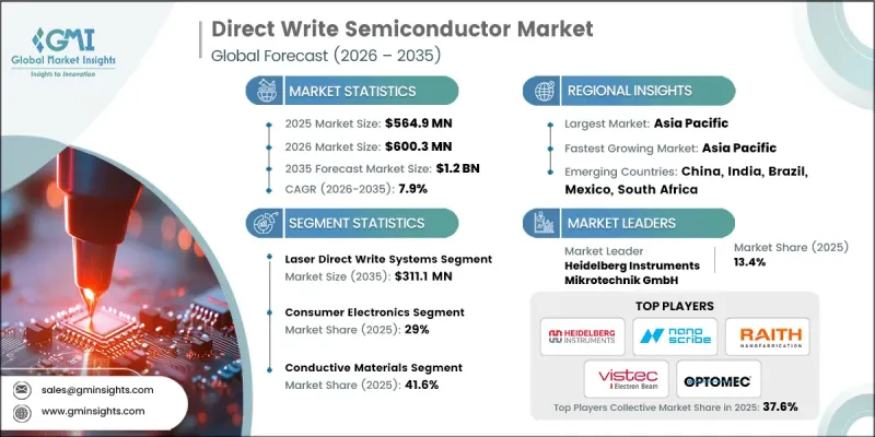
直接寫入式半導體產業的成長主要源自於對速度更快、精度更高、成本效益更高的半導體製造技術日益成長的需求。隨著製造商尋求能夠降低製造複雜性並提高設計柔軟性的替代方案,直接寫入式技術正蓬勃發展。無掩模光刻和先進的圖形化解決方案在這項變革中發揮核心作用,它們縮短了裝置開發週期並提高了製造精度。這些技術有助於半導體開發商加速原型製作流程、最大限度地減少材料損耗並提高製造工作流程的效率。此外,隨著向下一代電子設備的過渡不斷推進,市場對能夠支援緊湊型多功能組件設計的製造解決方案的需求也日益強勁。直接寫入式技術使製造商能夠以高精度沉積導電材料和半導體材料,從而開發出具有卓越解析度的複雜電路。這種能力也使研究人員和製造商能夠探索新的裝置架構和創新設計方案。直接寫入式半導體市場也受惠於混合製造方法的日益普及,這些方法將直接寫入式製程與傳統半導體製造技術結合。此類方法使製造商能夠創建具有增強功能的高度客製化的多層電子元件。此外,人們對按需製造和小批量生產的興趣日益濃厚,推動了直接寫入技術在研究環境和專業電子產品開發中的應用。
| 市場範圍 | |
|---|---|
| 開始年份 | 2025 |
| 預測期 | 2026-2035 |
| 上市時的市場規模 | 5.649億美元 |
| 預測金額 | 12億美元 |
| 複合年成長率 | 7.9% |
預計2035年,雷射直接照明系統市場規模將達到3.111億美元。基於雷射的直接照明系統因其卓越的精度、高速的處理能力和多樣化的圖形化能力而備受關注。這些系統使製造商能夠在微尺度上創建複雜的電路結構,而無需依賴傳統的掩模製造技術。直接在基板上產生複雜圖案的能力極大地提高了生產的柔軟性並縮短了開發週期。基於雷射的直接照明解決方案在先進電子製造領域尤其重要,因為它們支援快速原型製作,並允許在開發階段頻繁地進行設計變更。
預計到2025年,導電材料市佔率將達到41.6%,這反映了其在整個產業生態系統中的重要地位。導電材料在建構高精度電路和互連結構方面發揮著至關重要的作用,而這些結構對於現代電子元件至關重要。它們卓越的電氣性能、對各種基板的適應性以及與直接寫入製程的兼容性,使其成為從事先進微電子應用的製造商的理想選擇。隨著對高性能電子系統的關注度不斷提高,對能夠支援穩定可靠電路路徑的導電材料的需求也日益成長。此外,這些材料非常適合擴展直接寫入製造程序,因為它們能夠支援高效的電流傳輸並降低電阻。
預計2025年,歐洲直下式半導體市場規模將達9,640萬美元。隨著各地區政府日益重視提升國內半導體製造能力,歐洲直下式半導體產業正蓬勃發展。政策主導的措施正在促進技術創新,並支持整個全部區域先進半導體生產基礎設施的擴張。產業相關人員、研究機構和政府機構之間的策略合作也推動了下一代半導體製造技術的發展。這些努力旨在提高供應鏈韌性,增強技術競爭力,並支持半導體生態系統的長期成長。因此,先進的圖形化和積層製造技術的應用正在逐步擴展,從而鞏固了該地區在不斷發展的直下式半導體市場中的地位。
目錄
第1章:調查方法和範圍
第2章執行摘要
第3章業界考察
- 生態系分析
- 供應商情況
- 利潤率分析
- 成本結構
- 每個階段增加的價值
- 影響價值鏈的因素
- 中斷
- 影響產業的因素
- 促進因素
- 對先進客製化半導體解決方案的需求日益成長
- 拓展軟性、穿戴式和印刷電子產品的應用領域。
- 對快速原型製作和縮短產品上市時間的要求。
- 積層製造及其與先進材料的整合
- 用於半導體封裝的無掩模微影術技術取得進展
- 產業潛在風險與挑戰
- 較高的初始資本投資和設備成本
- 直接寫作過程的標準化程度有限。
- 市場機遇
- 採用異質整合和系統級封裝(SIP)
- 人工智慧驅動的流程最佳化和自動化
- 促進因素
- 監理情勢
- 北美洲
- 歐洲
- 亞太地區
- 拉丁美洲
- 中東和非洲
- 波特五力分析
- PESTEL 分析
- 科技與創新趨勢
- 當前技術趨勢
- 新興技術
- 新興經營模式
- 合規要求
- 專利和智慧財產權分析
- 地緣政治和貿易趨勢
第4章 競爭情勢
- 介紹
- 企業市佔率分析
- 按地區
- 北美洲
- 歐洲
- 亞太地區
- 拉丁美洲
- 中東和非洲
- 按地區
- 主要企業的競爭標竿分析
- 財務績效比較
- 銷售量
- 利潤率
- 研究與開發
- 產品系列比較
- 產品線寬度
- 科技
- 創新
- 區域擴張比較
- 全球擴張分析
- 服務網路覆蓋
- 按地區分類的市場滲透率
- 競爭定位矩陣
- 領導者
- 挑戰者
- 追蹤者
- 小眾玩家
- 戰略展望矩陣
- 財務績效比較
- 2021-2024 年重大發展
- 併購
- 夥伴關係和聯盟
- 技術進步
- 業務拓展與投資策略
- 數位轉型計劃
- 新興/Start-Ups競爭對手的發展趨勢
第5章 市場估算與預測:依技術/設備類型分類,2022-2035年
- 材料沉積系統
- 低黏度噴墨系統
- 中等黏度氣溶膠噴射系統
- 高黏度微量點膠系統
- 雷射直接光刻系統
- 空間燈光調變器(基於SLM/DMD)
- 直接雷射掃描系統
- 雙光子聚合系統
- 電子束直接微影系統
- 熱掃描探測器微影術系統
第6章 市場估算與預測:依材料類型分類,2022-2035年
- 導電材料
- 半導體材料
- 介電和絕緣材料
- 功能複合材料
第7章 市場估計與預測:依基板,2022-2035年
- 軟式電路板
- 剛性基板
- 保形/3D 基板
第8章 市場估計與預測:依應用領域分類,2022-2035年
- 先進的封裝與互連技術
- 軟性印刷電子
- 微機電系統和感測器
- 天線和射頻組件
- 生物醫學和醫療保健設備
- 其他
第9章 市場估計與預測:依最終用戶產業分類,2022-2035年
- 航太/國防
- 車
- 家用電子電器
- 醫療保健和醫療設備
- 通訊/5G
- 其他
第10章 市場估價與預測:依地區分類,2022-2035年
- 北美洲
- 美國
- 加拿大
- 歐洲
- 德國
- 英國
- 法國
- 西班牙
- 義大利
- 荷蘭
- 亞太地區
- 中國
- 印度
- 日本
- 澳洲
- 韓國
- 拉丁美洲
- 巴西
- 墨西哥
- 阿根廷
- 中東和非洲
- 南非
- 沙烏地阿拉伯
- 阿拉伯聯合大公國
第11章:公司簡介
- 主要企業
- Raith GmbH
- Heidelberg Instruments Mikrotechnik GmbH
- JEOL Ltd.
- Optomec Inc.
- 按地區分類的主要企業
- 北美洲
- NanoSystem Solutions, Inc.
- SVG Optronics Co., Ltd
- Nanoscribe GmbH &Co. KG
- 歐洲
- Vistec Electron Beam GmbH
- SUSS MicroTec SE
- Eulitha AG
- 亞太地區
- Elionix Inc.
- Crestec Corporation
- HTL Co. Japan Ltd.
- 北美洲
- 特殊玩家/干擾者
- KLOE SAS
- Holmarc Opto-Mechatronics Ltd.
- Microlight3D SAS
The Global Direct Write Semiconductor Market was valued at USD 564.9 million in 2025 and is estimated to grow at a CAGR of 7.9% to reach USD 1.2 billion by 2035.
Growth in the direct write semiconductor industry is largely driven by the increasing requirement for faster, highly accurate, and cost-efficient semiconductor manufacturing technologies. Direct write techniques are gaining momentum as manufacturers seek alternatives that improve design flexibility while reducing production complexity. Maskless lithography and advanced patterning solutions are playing a central role in this transformation by enabling faster device development cycles and improving manufacturing precision. These technologies help semiconductor developers accelerate prototyping processes, minimize material losses, and enhance the efficiency of fabrication workflows. In addition, the increasing shift toward next-generation electronic devices is creating a strong demand for manufacturing solutions capable of supporting compact and multifunctional component designs. Direct writing technology allows manufacturers to deposit conductive and semiconductive materials with high accuracy, enabling the development of complex circuits with superior resolution. This capability also allows researchers and manufacturers to explore new device architectures and innovative design possibilities. The direct write semiconductor market is also benefiting from the rising adoption of hybrid fabrication approaches that combine direct writing processes with traditional semiconductor production methods. Such approaches enable manufacturers to create highly customized and multi-layer electronic components with improved functionality. Furthermore, the increasing focus on on-demand manufacturing and limited-volume production is supporting the adoption of direct write technologies in research environments and specialized electronics development.
| Market Scope | |
|---|---|
| Start Year | 2025 |
| Forecast Year | 2026-2035 |
| Start Value | $564.9 Million |
| Forecast Value | $1.2 Billion |
| CAGR | 7.9% |
The laser direct write systems segment is projected to reach USD 311.1 million by 2035. Laser-based direct writing systems are gaining considerable attention due to their ability to deliver exceptional accuracy, high processing speed, and versatile patterning capabilities. These systems allow manufacturers to create intricate circuit structures at microscales without relying on conventional mask-based fabrication techniques. The ability to generate complex patterns directly on substrates significantly improves production flexibility and shortens development timelines. Laser-enabled direct writing solutions are particularly valuable in advanced electronics manufacturing because they support rapid prototyping and enable frequent design modifications during development stages.
The conductive materials segment accounted for 41.6% share in 2025, reflecting its significant importance within the overall industry ecosystem. Conductive materials play a vital role in the formation of high-precision circuits and interconnect structures that are essential for modern electronic components. Their strong electrical performance, adaptability across different substrate materials, and compatibility with direct writing processes make them a preferred choice for manufacturers working on advanced microelectronic applications. The increasing focus on high-performance electronic systems is further strengthening demand for conductive materials capable of supporting stable and reliable electrical pathways. In addition, the ability of these materials to support efficient current transmission and reduce electrical resistance makes them highly suitable for scaling direct write fabrication processes.
Europe Direct Write Semiconductor Market generated USD 96.4 million in 2025. The Europe direct write semiconductor industry is progressing as regional authorities place increasing emphasis on strengthening domestic semiconductor manufacturing capabilities. Policy-driven initiatives are encouraging technological innovation and supporting the expansion of advanced semiconductor production infrastructure across the region. Strategic collaboration among industry participants, research organizations, and government institutions is also contributing to the development of next-generation semiconductor fabrication technologies. These efforts are focused on improving supply chain resilience, enhancing technological competitiveness, and supporting long-term growth within the semiconductor ecosystem. As a result, the adoption of advanced patterning and additive manufacturing technologies is gradually expanding, reinforcing the region's role in the evolving direct write semiconductor market.
Key companies operating in the Global Direct Write Semiconductor Market include Raith GmbH, Vistec Electron Beam GmbH, Heidelberg Instruments Mikrotechnik GmbH, JEOL Ltd., Elionix Inc., SUSS MicroTec SE, Nanoscribe GmbH & Co. KG, Eulitha AG, Crestec Corporation, KLOE SAS, Holmarc Opto-Mechatronics Ltd., and HTL Co. Japan Ltd., Microlight3D SAS, NanoSystem Solutions, Inc., SVG Optronics Co., Ltd, and Optomec Inc. Companies active in the Global Direct Write Semiconductor Market are adopting several strategic initiatives to strengthen their competitive position and expand their technological capabilities. Many firms are increasing investment in research and development to enhance the precision, speed, and efficiency of direct writing technologies. Product innovation is another key strategy, with companies focusing on the development of advanced systems capable of supporting high-resolution semiconductor fabrication and complex circuit patterning. Strategic partnerships with research institutions and semiconductor manufacturers are also becoming more common as companies aim to accelerate technology development and expand commercial applications. Additionally, market participants are emphasizing the integration of advanced materials and software-driven design tools to improve system performance.
Table of Contents
Chapter 1 Methodology and Scope
- 1.1 Market scope and definition
- 1.2 Research design
- 1.2.1 Research approach
- 1.2.2 Data collection methods
- 1.3 Data mining sources
- 1.3.1 Global
- 1.3.2 Regional/Country
- 1.4 Base estimates and calculations
- 1.4.1 Base year calculation
- 1.4.2 Key trends for market estimation
- 1.5 Primary research and validation
- 1.5.1 Primary sources
- 1.6 Forecast model
- 1.7 Research assumptions and limitations
Chapter 2 Executive Summary
- 2.1 Industry 360° synopsis, 2021 - 2034
- 2.2 Key market trends
- 2.2.1 Technology/equipment type trends
- 2.2.2 Material type trends
- 2.2.3 Substrate trends
- 2.2.4 Application trends
- 2.2.5 End-user industry trends
- 2.2.6 Regional trends
- 2.3 TAM analysis, 2025-2034
- 2.4 CXO perspectives: Strategic imperatives
- 2.4.1 Executive decision points
- 2.4.2 Critical success factors
- 2.5 Future outlook and strategic recommendations
Chapter 3 Industry Insights
- 3.1 Industry ecosystem analysis
- 3.1.1 Supplier landscape
- 3.1.2 Profit margin analysis
- 3.1.3 Cost structure
- 3.1.4 Value addition at each stage
- 3.1.5 Factor affecting the value chain
- 3.1.6 Disruptions
- 3.2 Industry impact forces
- 3.2.1 Growth drivers
- 3.2.1.1 Increasing demand for advanced and custom semiconductor solutions
- 3.2.1.2 Expansion of flexible, wearable, and printed electronics applications
- 3.2.1.3 Rapid prototyping and reduced time-to-market requirements
- 3.2.1.4 Integration with additive manufacturing and advanced materials
- 3.2.1.5 Advancement in maskless lithography technologies for semiconductor packaging
- 3.2.2 Industry pitfalls and challenges
- 3.2.2.1 High initial capital expenditure and equipment costs
- 3.2.2.2 Limited standardization of direct writing processes
- 3.2.3 Market opportunities
- 3.2.3.1 Adoption in heterogeneous integration and system-in-package (SIP)
- 3.2.3.2 AI-enabled process optimization and automation
- 3.2.1 Growth drivers
- 3.3 Regulatory landscape
- 3.3.1 North America
- 3.3.2 Europe
- 3.3.3 Asia Pacific
- 3.3.4 Latin America
- 3.3.5 Middle East & Africa
- 3.4 Porter's analysis
- 3.5 PESTEL analysis
- 3.6 Technology and innovation landscape
- 3.6.1 Current technological trends
- 3.6.2 Emerging technologies
- 3.7 Emerging business models
- 3.8 Compliance requirements
- 3.9 Patent and IP analysis
- 3.10 Geopolitical and trade dynamics
Chapter 4 Competitive Landscape, 2024
- 4.1 Introduction
- 4.2 Company market share analysis
- 4.2.1 By region
- 4.2.1.1 North America
- 4.2.1.2 Europe
- 4.2.1.3 Asia Pacific
- 4.2.1.4 Latin America
- 4.2.1.5 Middle East & Africa
- 4.2.1 By region
- 4.3 Competitive benchmarking of key players
- 4.3.1 Financial performance comparison
- 4.3.1.1 Revenue
- 4.3.1.2 Profit margin
- 4.3.1.3 R&D
- 4.3.2 Product portfolio comparison
- 4.3.2.1 Product range breadth
- 4.3.2.2 Technology
- 4.3.2.3 Innovation
- 4.3.3 Geographic presence comparison
- 4.3.3.1 Global footprint analysis
- 4.3.3.2 Service network coverage
- 4.3.3.3 Market penetration by region
- 4.3.4 Competitive positioning matrix
- 4.3.4.1 Leaders
- 4.3.4.2 Challengers
- 4.3.4.3 Followers
- 4.3.4.4 Niche players
- 4.3.5 Strategic outlook matrix
- 4.3.1 Financial performance comparison
- 4.4 Key developments, 2021-2024
- 4.4.1 Mergers and acquisitions
- 4.4.2 Partnerships and collaborations
- 4.4.3 Technological advancements
- 4.4.4 Expansion and investment strategies
- 4.4.5 Digital transformation initiatives
- 4.5 Emerging/ startup competitors landscape
Chapter 5 Market Estimates and Forecast, By Technology / Equipment Type, 2022 - 2035 ($ Mn)
- 5.1 Key trends
- 5.2 Material deposition systems
- 5.2.1 Low-viscosity inkjet systems
- 5.2.2 Medium-viscosity aerosol jet systems
- 5.2.3 High-viscosity micro-dispensing systems
- 5.3 Laser direct write systems
- 5.3.1 Spatial light modulator (SLM/DMD-Based)
- 5.3.2 Direct laser scanning systems
- 5.3.3 Two-photon polymerization systems
- 5.4 Electron beam direct write systems
- 5.5 Thermal scanning probe lithography systems
Chapter 6 Market Estimates and Forecast, By Material Type, 2022 - 2035 ($ Mn)
- 6.1 Key trends
- 6.2 Conductive materials
- 6.3 Semiconductor materials
- 6.4 Dielectric & insulating materials
- 6.5 Functional composite materials
Chapter 7 Market Estimates and Forecast, By Substrate, 2022 - 2035 ($ Mn)
- 7.1 Key trends
- 7.2 Flexible substrates
- 7.3 Rigid substrates
- 7.4 Conformal/3D substrates
Chapter 8 Market Estimates and Forecast, By Application, 2022 - 2035 ($ Mn)
- 8.1 Key trends
- 8.2 Advanced packaging & interconnects
- 8.3 Flexible & printed electronics
- 8.4 Mems & sensors
- 8.5 Antennas & RF components
- 8.6 Biomedical & healthcare devices
- 8.7 Others
Chapter 9 Market Estimates and Forecast, By End-User Industry, 2022 - 2035 ($ Mn)
- 9.1 Key trends
- 9.2 Aerospace & defense
- 9.3 Automotive
- 9.4 Consumer electronics
- 9.5 Healthcare & medical devices
- 9.6 Telecommunications & 5G
- 9.7 Others
Chapter 10 Market Estimates and Forecast, By Region, 2022 - 2035 ($ Mn)
- 10.1 Key trends
- 10.2 North America
- 10.2.1 U.S.
- 10.2.2 Canada
- 10.3 Europe
- 10.3.1 Germany
- 10.3.2 UK
- 10.3.3 France
- 10.3.4 Spain
- 10.3.5 Italy
- 10.3.6 Netherlands
- 10.4 Asia Pacific
- 10.4.1 China
- 10.4.2 India
- 10.4.3 Japan
- 10.4.4 Australia
- 10.4.5 South Korea
- 10.5 Latin America
- 10.5.1 Brazil
- 10.5.2 Mexico
- 10.5.3 Argentina
- 10.6 Middle East and Africa
- 10.6.1 South Africa
- 10.6.2 Saudi Arabia
- 10.6.3 UAE
Chapter 11 Company Profiles
- 11.1 Global Key Players
- 11.1.1 Raith GmbH
- 11.1.2 Heidelberg Instruments Mikrotechnik GmbH
- 11.1.3 JEOL Ltd.
- 11.1.4 Optomec Inc.
- 11.2 Regional Key Players
- 11.2.1 North America
- 11.2.1.1 NanoSystem Solutions, Inc.
- 11.2.1.2 SVG Optronics Co., Ltd
- 11.2.1.3 Nanoscribe GmbH & Co. KG
- 11.2.2 Europe
- 11.2.2.1 Vistec Electron Beam GmbH
- 11.2.2.2 SUSS MicroTec SE
- 11.2.2.3 Eulitha AG
- 11.2.3 APAC
- 11.2.3.1 Elionix Inc.
- 11.2.3.2 Crestec Corporation
- 11.2.3.3 HTL Co. Japan Ltd.
- 11.2.1 North America
- 11.3 Niche Players / Disruptors
- 11.3.1 KLOE SAS
- 11.3.2 Holmarc Opto-Mechatronics Ltd.
- 11.3.3 Microlight3D SAS
 光敏三極管市場報告:趨勢、預測與競爭分析(至2035年)
 導線架市場:2026-2032年全球市場預測(依材料、層結構、製程、引線數量、佈線方式、板材覆蓋率、應用和最終用戶分類)半導體二極體市場:按類型、封裝、材料、銷售管道、額定電壓、額定電流、應用和最終用戶產業分類-2026-2032年全球市場預測
 2026年全球主動半導體盤式雷射市場報告半導體排氣系統市場:依排氣技術、組件、晶圓尺寸、應用、最終用戶、安裝類型和銷售管道-全球預測,2026-2032年自動化FOUP開啟器市場:依晶圓尺寸、類型、自動化程度、連接方式和最終用戶產業分類-2026-2032年全球預測高純度介質供應系統市場:依介質類型、純度等級、銷售管道和應用分類-全球預測,2026-2032年
 用於替代能源技術的半導體:機會和市場全球自動化半導體封裝機械市場(按機器類型、技術、應用和最終用戶分類)預測(2026-2032年)PGMEA半導體市場按等級、應用和最終用途行業分類,全球預測,2026-2032年