

 |
市場調查報告書
商品編碼
1998729
氮化鎵基板市場機會、成長要素、產業趨勢分析及2026-2035年預測GaN Substrate Market Opportunity, Growth Drivers, Industry Trend Analysis, and Forecast 2026 - 2035 |
||||||
預計到 2025 年,全球 GaN基板市場價值將達到 2.923 億美元,並預計以 11.5% 的複合年成長率成長,到 2035 年達到 8.612 億美元。
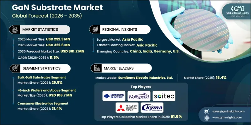
市場需求的激增主要得益於氮化鎵(GaN)基板在電動車和電力電子領域的應用日益廣泛,以及5G和即將到來的6G通訊基礎設施的快速部署。 GaN基板具有卓越的溫度控管、高效率和高耐壓性能,是小型逆變器、轉換器和車載充電器的關鍵材料。其在高效能LED、光電元件、資料中心和可再生能源系統等領域的廣泛應用也進一步推動了市場成長。汽車、通訊和家用電子電器產業對更小巧、更節能裝置的需求不斷成長,促使製造商整合GaN技術,從而在提升裝置性能的同時,降低能耗和面積。強大的研發投入以及對高可靠性基板的需求,正在加速全球市場的普及。 GaN基板在電力電子和電動車(EV)領域的日益普及是市場成長的主要驅動力。與傳統的矽基元件相比,GaN基板具有更高的效率、更優異的熱穩定性和更高的耐壓性能,能夠更好地支援小型逆變器、轉換器和車載充電器等應用。此外,GaN基板能夠實現高頻、高功率和節能的射頻組件,而5G的普及和6G網路的部署正在加速需求。
| 市場範圍 | |
|---|---|
| 開始年份 | 2025 |
| 預測期 | 2026-2035 |
| 初始市場規模 | 2.923億美元 |
| 預計金額 | 8.612億美元 |
| 複合年成長率 | 11.5% |
體氮化鎵基板憑藉其卓越的晶體品質、優異的導熱性和幾乎無缺陷的結構,預計到2025年將佔據29.5%的市場佔有率。這些特性使其成為高性能工業、汽車和通訊應用的理想選擇,在這些應用中,可靠性、效率和長期耐久性至關重要。體氮化鎵基板能夠在高壓和高溫環境下保持穩定性,使製造商能夠生產出結構緊湊、節能高效且使用壽命更長的裝置。隨著電力電子、射頻元件和光電子系統對更高性能和小型化的需求不斷成長,體氮化鎵基板製造商 (OEM) 和整合商的最佳選擇。
預計2025年,大直徑晶圓,尤其是6吋以上尺寸的晶圓,市場規模將達到1.067億美元。其受歡迎的原因在於,它們能夠實現大規模生產,同時提高產量比率並降低單位製造成本。這些晶圓對於電力電子、可再生能源系統和高頻通訊設備等應用的規模化至關重要。其尺寸允許在單個晶圓上製造多個裝置,從而最佳化資源利用率並提高成本效益。隨著各行業對更大、更有效率、更可靠的組件的需求不斷成長,對大直徑GaN晶圓的需求也持續穩定成長。
預計到2025年,北美氮化鎵基板市佔率將達到28.6%。這一成長主要得益於該地區電動車、工業功率模組和可再生能源系統的快速普及,以及5G和下一代6G基礎設施的部署。強大的研發能力、先進的晶圓製造技術以及對下一代功率電子技術的早期應用,都鞏固了該地區的主導地位。此外,國防現代化計畫、航太電子和雷達應用也進一步加速了氮化鎵基板的普及。這些因素,加上主要企業的策略性投資和扶持性產業政策,持續鞏固了北美作為氮化鎵基板市場主導中心的地位。
目錄
第1章:調查方法和範圍
第2章執行摘要
第3章業界考察
- 生態系分析
- 供應商情況
- 利潤率
- 成本結構
- 每個階段增加的價值
- 影響價值鏈的因素
- 中斷
- 影響產業的因素
- 促進因素
- 氮化鎵基板在電力電子和電動車領域的應用日益廣泛
- 擴大5G/6G和高頻通訊基礎設施部署
- 對高效率發光二極體和光電元件的需求日益成長
- 資料中心和可再生能源系統的擴展需要高效的電力轉換。
- 氮化鎵晶圓生長和大直徑晶圓生產的技術進步。
- 產業潛在風險與挑戰
- 高昂的製造成本和複雜的生產流程
- 大尺寸、無缺陷氮化鎵基板供不應求
- 促進因素
- 成長潛力分析
- 監理情勢
- 北美洲
- 歐洲
- 亞太地區
- 拉丁美洲
- 中東和非洲
- 波特五力分析
- PESTEL 分析
- 科技與創新趨勢
- 當前技術趨勢
- 新興技術
- 價格趨勢
- 按地區
- 依產品
- 定價策略
- 新興經營模式
- 合規要求
- 專利和智慧財產權分析
第4章 競爭情勢
- 介紹
- 企業市佔率分析
- 按地區
- 北美洲
- 歐洲
- 亞太地區
- 拉丁美洲
- 中東和非洲
- 市場集中度分析
- 按地區
- 主要企業的競爭標竿分析
- 財務績效比較
- 銷售量
- 利潤率
- 研究與開發
- 產品系列比較
- 產品線寬度
- 科技
- 創新
- 區域擴張比較
- 全球擴張分析
- 服務網路覆蓋
- 按地區分類的市場滲透率
- 競爭定位矩陣
- 領導者
- 挑戰者
- 追蹤者
- 小眾玩家
- 財務績效比較
- 主要進展
- 併購
- 夥伴關係和聯盟
- 技術進步
- 業務拓展與投資策略
- 數位轉型計劃
- 新興競爭對手和Start-Ups競爭對手的發展趨勢
第5章 市場估算與預測:依基板類型分類,2022-2035年
- GaN/SiC(碳化矽)基板
- GaN-on-Si(矽)基板
- 藍寶石基板上的氮化鎵
- 體氮化鎵基板
- 其他
第6章 依晶圓尺寸分類的市場估算與預測,2022-2035年
- 小於 2 英吋的晶圓
- 4吋晶圓
- 6吋晶圓
- 小於 6 英吋和大於 6 英吋的晶圓
第7章 市場估計與預測:依應用領域分類,2022-2035年
- LED
- 電力電子
- 射頻(RF)設備
- 雷射二極體
- 檢測器
- MEMS元件
- 太陽能電池
- 感應器
- 其他
第8章 市場估算與預測:依最終用途產業分類,2022-2035年
- 家用電子電器
- 溝通
- 車
- 航太/國防
- 衛生保健
- 能源與電力
- 其他
第9章 市場估計與預測:依地區分類,2022-2035年
- 北美洲
- 美國
- 加拿大
- 歐洲
- 德國
- 英國
- 法國
- 西班牙
- 義大利
- 荷蘭
- 亞太地區
- 中國
- 印度
- 日本
- 澳洲
- 韓國
- 拉丁美洲
- 巴西
- 墨西哥
- 阿根廷
- 中東和非洲
- 南非
- 沙烏地阿拉伯
- 阿拉伯聯合大公國
第10章:公司簡介
- 主要企業
- Sumitomo Electric Industries, Ltd.
- Mitsubishi Chemical Group Corporation
- Nichia Corporation
- Qorvo
- Wolfspeed
- Soitec
- Infineon Technologies
- STMicroelectronics
- NXP Semiconductors
- 按地區分類的主要企業
- DOWA Electronics Materials Co., Ltd.
- Okmetic
- Kyma Technologies Inc
- Rohm Semiconductor
- TDK Corporation
- 特殊玩家/干擾者
- Coherent
The Global GaN Substrate Market was valued at USD 292.3 million in 2025 and is estimated to grow at a CAGR of 11.5% to reach USD 861.2 million by 2035.
The surge in market demand is driven by the increasing adoption of GaN substrates in electric vehicles and power electronics, along with growing deployment of 5G and upcoming 6G telecommunications infrastructure. GaN substrates offer superior thermal management, higher efficiency, and elevated breakdown voltage, making them essential for compact inverters, converters, and onboard chargers. Expanding applications in high-efficiency LEDs, optoelectronic devices, data centers, and renewable energy systems are further fueling growth. The rising need for smaller, energy-efficient devices across automotive, telecom, and consumer electronics sectors is driving manufacturers to integrate GaN technology, enhancing device performance while reducing energy losses and footprint. Strong R&D, coupled with demand for high-reliability substrates, is reinforcing market adoption worldwide. The increasing use of GaN substrates in power electronics and electric vehicles is a major market driver. These substrates enable higher efficiency, improved thermal stability, and elevated breakdown voltage, supporting compact inverters, converters, and onboard EV chargers compared to traditional silicon-based devices. The adoption of 5G and the anticipated rollout of 6G networks are also accelerating demand, as GaN substrates enable high-frequency, high-power, and energy-efficient RF components.
| Market Scope | |
|---|---|
| Start Year | 2025 |
| Forecast Year | 2026-2035 |
| Start Value | $292.3 Million |
| Forecast Value | $861.2 Million |
| CAGR | 11.5% |
The bulk GaN substrates segment held a 29.5% share in 2025, due to their exceptional crystalline quality, superior thermal conductivity, and nearly defect-free structure. These characteristics make them ideal for high-performance industrial, automotive, and telecom applications, where reliability, efficiency, and long-term durability are critical. Their ability to handle high voltages and temperatures while maintaining stability allows manufacturers to produce compact, energy-efficient devices with enhanced operational lifespans. As power electronics, RF devices, and optoelectronic systems increasingly demand higher performance and smaller footprints, bulk GaN substrates remain the preferred choice for OEMs and integrators seeking consistent quality and performance.
The large-diameter wafers, particularly those above 6 inches segment reached USD 106.7 million in 2025. Their popularity stems from the ability to enable high-volume manufacturing while improving yield rates and lowering per-unit production costs. These wafers are essential for scaling applications in power electronics, renewable energy systems, and high-frequency telecom devices. Their size allows multiple devices to be fabricated on a single wafer, optimizing resource utilization and cost efficiency. As industries push for larger, high-efficiency, and more reliable components, demand for large-diameter GaN wafers continues to grow steadily.
North America GaN Substrate Market accounted for 28.6% share in 2025, driven by the region's rapid adoption of electric vehicles, industrial power modules, renewable energy systems, and deployment of 5G and emerging 6G infrastructure. Strong R&D capabilities, advanced wafer fabrication technologies, and early adoption of next-generation power electronics contribute to regional leadership. Additionally, defense modernization programs, aerospace electronics, and radar applications further accelerate the uptake of GaN substrates. These factors, combined with strategic investments from key players and supportive industrial policies, continue to strengthen North America's position as a dominant hub in the GaN substrate market.
Key players in the GaN Substrate Market include Coherent, DOWA Electronics Materials Co., Ltd., Infineon Technologies, Kyma Technologies Inc., Mitsubishi Chemical Group Corporation, Nichia Corporation, NXP Semiconductors, Okmetic, Qorvo, Rohm Semiconductor, Samsung Electronics, Soitec, STMicroelectronics, Sumitomo Electric Industries, Ltd., TDK Corporation, and Wolfspeed. Companies operating in the GaN Substrate Market are implementing multiple strategies to strengthen their market foothold. Many are investing heavily in R&D to develop higher-quality, defect-free bulk substrates and large-diameter wafers, improving performance for automotive, telecom, and industrial applications. Strategic partnerships with electric vehicle manufacturers, telecom companies, and renewable energy integrators are expanding adoption across high-growth segments. Several players are pursuing technology collaborations to enhance substrate efficiency and thermal performance while reducing production costs. Global expansion initiatives, including localized wafer production and strategic alliances with distributors, are helping reach emerging markets faster.
Table of Contents
Chapter 1 Methodology and Scope
- 1.1 Market scope and definition
- 1.2 Research design
- 1.2.1 Research approach
- 1.2.2 Data collection methods
- 1.3 Data mining sources
- 1.3.1 Global
- 1.3.2 Regional/Country
- 1.4 Base estimates and calculations
- 1.4.1 Base year calculation
- 1.4.2 Key trends for market estimation
- 1.5 Primary research and validation
- 1.5.1 Primary sources
- 1.6 Forecast model
- 1.7 Research assumptions and limitations
Chapter 2 Executive Summary
- 2.1 Industry 360° synopsis, 2022 - 2035
- 2.2 Key market trends
- 2.2.1 Substrate Type trends
- 2.2.2 Wafer Size trends
- 2.2.3 Application trends
- 2.2.4 End-use Industry trends
- 2.2.5 Regional trends
- 2.3 TAM Analysis, 2026-2035
- 2.4 CXO perspectives: Strategic imperatives
Chapter 3 Industry Insights
- 3.1 Industry ecosystem analysis
- 3.1.1 Supplier Landscape
- 3.1.2 Profit Margin
- 3.1.3 Cost structure
- 3.1.4 Value addition at each stage
- 3.1.5 Factor affecting the value chain
- 3.1.6 Disruptions
- 3.2 Industry impact forces
- 3.2.1 Growth drivers
- 3.2.1.1 Increasing adoption of GaN substrates in power electronics and electric vehicles
- 3.2.1.2 Growing deployment of 5G/6G and high-frequency telecommunications infrastructure
- 3.2.1.3 Rising demand for high-efficiency LEDs and optoelectronic devices
- 3.2.1.4 Expansion of data centers and renewable energy systems requiring efficient power conversion
- 3.2.1.5 Technological advancements in GaN wafer growth and large-diameter wafer production
- 3.2.2 Industry pitfalls and challenges
- 3.2.2.1 High manufacturing cost and complex production processes
- 3.2.2.2 Limited availability of large-size, defect-free GaN substrates
- 3.2.1 Growth drivers
- 3.3 Growth potential analysis
- 3.4 Regulatory landscape
- 3.4.1 North America
- 3.4.2 Europe
- 3.4.3 Asia Pacific
- 3.4.4 Latin America
- 3.4.5 Middle East & Africa
- 3.5 Porter's analysis
- 3.6 PESTEL analysis
- 3.7 Technology and Innovation landscape
- 3.7.1 Current technological trends
- 3.7.2 Emerging technologies
- 3.8 Price trends
- 3.8.1 By region
- 3.8.2 By product
- 3.9 Pricing strategies
- 3.10 Emerging business models
- 3.11 Compliance requirements
- 3.12 Patent and IP analysis
Chapter 4 Competitive Landscape, 2025
- 4.1 Introduction
- 4.2 Company market share analysis
- 4.2.1 By region
- 4.2.1.1 North America
- 4.2.1.2 Europe
- 4.2.1.3 Asia Pacific
- 4.2.1.4 Latin America
- 4.2.1.5 Middle East & Africa
- 4.2.2 Market concentration analysis
- 4.2.1 By region
- 4.3 Competitive benchmarking of key players
- 4.3.1 Financial performance comparison
- 4.3.1.1 Revenue
- 4.3.1.2 Profit margin
- 4.3.1.3 R&D
- 4.3.2 Product portfolio comparison
- 4.3.2.1 Product range breadth
- 4.3.2.2 Technology
- 4.3.2.3 Innovation
- 4.3.3 Geographic presence comparison
- 4.3.3.1 Global footprint analysis
- 4.3.3.2 Service network coverage
- 4.3.3.3 Market penetration by region
- 4.3.4 Competitive positioning matrix
- 4.3.4.1 Leaders
- 4.3.4.2 Challengers
- 4.3.4.3 Followers
- 4.3.4.4 Niche players
- 4.3.1 Financial performance comparison
- 4.4 Key developments
- 4.4.1 Mergers and acquisitions
- 4.4.2 Partnerships and collaborations
- 4.4.3 Technological advancements
- 4.4.4 Expansion and investment strategies
- 4.4.5 Digital transformation initiatives
- 4.5 Emerging/ startup competitors landscape
Chapter 5 Market Estimates and Forecast, By Substrate Type, 2022 - 2035 (USD Million)
- 5.1 Key trends
- 5.2 GaN-on-SiC (Silicon Carbide) substrates
- 5.3 GaN-on-Si (Silicon) substrates
- 5.4 GaN-on-Sapphire substrates
- 5.5 Bulk GaN substrates
- 5.6 Others
Chapter 6 Market Estimates and Forecast, By Wafer Size, 2022 - 2035 (USD Million)
- 6.1 Key trends
- 6.2 < 2-inch wafers
- 6.3 4-inch wafers
- 6.4 6-inch wafers
- 6.5 <6-inch wafers and above
Chapter 7 Market Estimates and Forecast, By Application, 2022 - 2035 (USD Million)
- 7.1 Key trends
- 7.2 LEDs
- 7.3 Power electronics
- 7.4 Radio frequency (RF) devices
- 7.5 Laser diodes
- 7.6 Photodetectors
- 7.7 MEMS devices
- 7.8 Solar cells
- 7.9 Sensors
- 7.10 Others
Chapter 8 Market Estimates and Forecast, By End-use Industry, 2022 - 2035 (USD Million)
- 8.1 Key trends
- 8.2 Consumer electronics
- 8.3 Telecommunications
- 8.4 Automotive
- 8.5 Aerospace & defense
- 8.6 Healthcare
- 8.7 Energy & power
- 8.8 Others
Chapter 9 Market Estimates and Forecast, By Region, 2022 - 2035 (USD Million)
- 9.1 Key trends
- 9.2 North America
- 9.2.1 U.S.
- 9.2.2 Canada
- 9.3 Europe
- 9.3.1 Germany
- 9.3.2 UK
- 9.3.3 France
- 9.3.4 Spain
- 9.3.5 Italy
- 9.3.6 Netherlands
- 9.4 Asia Pacific
- 9.4.1 China
- 9.4.2 India
- 9.4.3 Japan
- 9.4.4 Australia
- 9.4.5 South Korea
- 9.5 Latin America
- 9.5.1 Brazil
- 9.5.2 Mexico
- 9.5.3 Argentina
- 9.6 Middle East and Africa
- 9.6.1 South Africa
- 9.6.2 Saudi Arabia
- 9.6.3 UAE
Chapter 10 Company Profiles
- 10.1 Global Key Players
- 10.1.1 Sumitomo Electric Industries, Ltd.
- 10.1.2 Mitsubishi Chemical Group Corporation
- 10.1.3 Nichia Corporation
- 10.1.4 Qorvo
- 10.1.5 Wolfspeed
- 10.1.6 Soitec
- 10.1.7 Infineon Technologies
- 10.1.8 STMicroelectronics
- 10.1.9 NXP Semiconductors
- 10.2 Regional key players
- 10.2.1 DOWA Electronics Materials Co., Ltd.
- 10.2.2 Okmetic
- 10.2.3 Kyma Technologies Inc
- 10.2.4 Rohm Semiconductor
- 10.2.5 TDK Corporation
- 10.3 Niche Players/Disruptors
- 10.3.1 Coherent
 2026-2034年全球氮化鎵基板市場規模、佔有率、趨勢和成長分析報告
 按直徑、晶體取向、製造方法、應用和終端用戶產業分類的氮化鎵單晶基板市場—2026-2032年全球預測氮化鎵半導體元件及基板晶圓市場(按元件類型、基板、晶圓尺寸、應用和銷售管道)——2026-2032年全球預測氮化鎵基板市場按元件應用、基板材料、晶圓直徑、外延技術、晶體取向、摻雜類型、最終用戶和分銷管道分類-2026-2032年全球預測氮化鎵(GaN)基板市場:2025-2030年預測
 全球GaN基板市場
 鑽石半導體基板上的GaN市場- 成長,未來展望,競爭分析,2024年~2032年