

 |
市場調查報告書
商品編碼
1982387
SiC晶圓回收服務市場:商業機會、成長要素、產業趨勢分析及2026-2035年預測。SiC Wafer Reclaim Services Market Opportunity, Growth Drivers, Industry Trend Analysis, and Forecast 2026 - 2035 |
||||||
全球碳化矽晶圓回收服務市場預計到 2025 年將達到 6.84 億美元,年複合成長率為 8.4%,到 2035 年將達到 15 億美元。
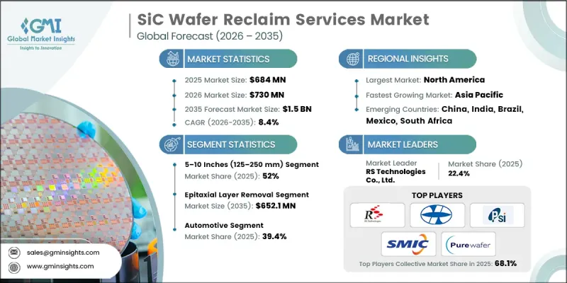
這一成長主要得益於電動車 (EV) 的快速普及,從而提升了對碳化矽 (SiC) 基功率裝置的需求,這些裝置廣泛應用於牽引逆變器、車載充電器和電源管理系統等領域。這些裝置因其高效率、優異的產量比率性和耐壓性而備受青睞。政府支持半導體製造的各項舉措,包括獎勵、補貼和晶圓廠擴建計劃,進一步推動了晶圓回收服務的需求。晶圓回收已成為一項至關重要且經濟高效的製造策略,能夠提高良率並減少材料廢棄物。晶圓直徑不斷增大,尤其是 150 毫米和 200 毫米晶圓,這需要先進的拋光、偵測和表面特性分析工具。服務供應商正在整合先進的測量和污染控制技術,以提供高品質的回收晶圓,滿足汽車和工業電力電子領域日益嚴格的平整度和缺陷接受度要求。
| 市場範圍 | |
|---|---|
| 開始年份 | 2025 |
| 預測期 | 2026-2035 |
| 上市時的市場規模 | 6.84億美元 |
| 預測金額 | 15億美元 |
| 複合年成長率 | 8.4% |
上文提到的10吋(超過250毫米)晶圓市場預計將在2026年至2035年間以8.9%的複合年成長率成長。超大尺寸晶圓對於下一代功率元件至關重要,但其加工需要專用設備、精確的層去除和先進的拋光技術,以防止開裂、翹曲或污染。製造商正在改進這些工藝,以最大限度地減少材料損失、降低生產成本,並支援碳化矽元件在汽車、工業和能源領域的大規模應用。
預計到2025年,研磨和拋光服務市場規模將達到1.681億美元,並在2026年至2035年間以8.8%的複合年成長率成長。這些服務專注於實現碳化矽晶圓的高精度平整度、厚度和表面光滑度。自動化、製程監控和先進拋光材料的使用正日益廣泛地應用於提高產量比率、最大限度地減少晶圓間差異並增強製程一致性。客製化的研磨和拋光解決方案正被應用於滿足高功率電動車模組、工業轉換器和其他特殊應用的需求,使晶圓廠能夠在降低成本的同時交付可靠的晶圓。
預計2025年,北美碳化矽晶圓回收服務市佔率將達33.6%。該地區受益於成熟的半導體生態系統、碳化矽元件在汽車和工業領域的高滲透率以及先進的研究基礎設施。此外,美國和加拿大對清潔能源的重視也進一步推動了市場成長。
目錄
第1章:調查方法和範圍
第2章執行摘要
第3章業界考察
- 生態系分析
- 供應商情況
- 利潤率分析
- 成本結構
- 每個階段增加的價值
- 影響價值鏈的因素
- 中斷
- 影響產業的因素
- 促進因素
- 家用電子電器。
- 半導體在太陽能發電領域的應用日益廣泛
- SiC晶圓在5G和物聯網設備中的廣泛應用
- 電動車(EV)的廣泛普及
- 政府主導的擴大半導體製造規模的舉措日益增多
- 產業潛在風險與挑戰
- 製造工廠維修成本高昂
- 高產產量比率回收製程的技術挑戰
- 市場機遇
- 進入新興電動車製造地和新工廠
- 開發針對先進功率設備的優質回收服務
- 促進因素
- 監理情勢
- 北美洲
- 歐洲
- 亞太地區
- 拉丁美洲
- 中東和非洲
- 波特的分析
- PESTEL 分析
- 科技與創新趨勢
- 當前技術趨勢
- 新興技術
- 新興經營模式
- 合規要求
- 專利和智慧財產權分析
- 地緣政治和貿易趨勢
第4章 競爭情勢
- 介紹
- 企業市佔率分析
- 按地區
- 北美洲
- 歐洲
- 亞太地區
- 拉丁美洲
- 中東和非洲
- 按地區
- 主要企業的競爭標竿分析
- 財務績效比較
- 銷售量
- 利潤率
- 研究與開發
- 產品系列比較
- 產品線寬度
- 科技
- 創新
- 區域部署對比
- 全球擴張分析
- 服務網路覆蓋
- 按地區分類的市場滲透率
- 競爭定位矩陣
- 領導者
- 挑戰者
- 追蹤者
- 小眾玩家
- 財務績效比較
- 2022-2025 年重大發展
- 併購
- 夥伴關係和聯盟
- 技術進步
- 業務拓展與投資策略
- 數位轉型計劃
- 新興/Start-Ups競爭對手的發展趨勢
第5章 市場估算與預測:服務類型,2022-2035年
- 外延層去除
- 研磨和拋光服務
- 化學機械拋光(CMP)
- 表面拋光服務
- 清潔和檢查服務
- 其他
第6章 市場估算與預測:依晶圓直徑分類,2022-2035年
- 小於 5 英吋(100-125 毫米)
- 5-10吋(125-250毫米)
- 超過 10 吋(超過 250 毫米)
第7章 市場估計與預測:依復甦階段分類,2022-2035年
- 外延後回收
- 設備製造後的翻新
- 測試和品管後的再生
- 未使用晶圓的回收利用
第8章 市場估算與預測:依最終用途分類,2022-2035年
- 車
- 工業和製造業
- 通訊和資料中心
- 家用電子電器
- 可再生能源
- 航太/國防
- 其他
第9章 市場估價與預測:依最終用戶分類,2022-2035年
- 半導體製造商(IDM)
- 鑄造廠和契約製造
- 研究與發展機構與大學
- 晶圓經銷商和仲介業者
第10章 市場估價與預測:依地區分類,2022-2035年
- 北美洲
- 美國
- 加拿大
- 歐洲
- 德國
- 英國
- 法國
- 西班牙
- 義大利
- 荷蘭
- 亞太地區
- 中國
- 印度
- 日本
- 澳洲
- 韓國
- 拉丁美洲
- 巴西
- 墨西哥
- 阿根廷
- 中東和非洲
- 南非
- 沙烏地阿拉伯
- 阿拉伯聯合大公國
第11章:公司簡介
- 主要企業
- RS Technologies Co., Ltd.
- Phoenix Silicon International Corporation
- Semiconductor Industry Co., Ltd.
- Pure Wafer
- 按地區分類的主要企業
- Mimasu
- TOPCO Scientific
- Scientech Corporation
- 特殊玩家/干擾者
- Kinik Company
- NOVA Electronic Materials, LLC
- Silicon Materials Inc.
- GlobalWafers Co., Ltd.
- II-VI Incorporated
- STMicroelectronics
- ROHM Co., Ltd.
- Wolfspeed, A Cree Company
- Norstel AB
- GT Advanced Technologies
- DOWA Electronics Materials Co., Ltd.
- Siltronic AG
- Wafer World Inc.
The Global SiC Wafer Reclaim Services Market was valued at USD 684 million in 2025 and is estimated to grow at a CAGR of 8.4% to reach USD 1.5 billion by 2035.
The growth is fueled by the rapid adoption of electric vehicles (EVs), which is increasing demand for silicon carbide-based power devices in applications like traction inverters, onboard chargers, and power management systems. These devices are preferred for their high efficiency, excellent thermal tolerance, and voltage handling capabilities. Government initiatives supporting semiconductor manufacturing, including incentives, subsidies, and fab expansion programs, are further driving demand for wafer reclaim services. Reclaiming wafers has become an essential cost-efficient manufacturing strategy, enabling higher yields and reduced material waste. There is a growing trend toward larger diameter wafers, particularly 150 mm and 200 mm, which requires advanced polishing, inspection, and surface characterization tools. Service providers are integrating sophisticated metrology and contamination control techniques to ensure high-quality reclaimed wafers that meet increasingly stringent flatness and defect tolerance requirements for automotive and industrial power electronics.
| Market Scope | |
|---|---|
| Start Year | 2025 |
| Forecast Year | 2026-2035 |
| Start Value | $684 Million |
| Forecast Value | $1.5 Billion |
| CAGR | 8.4% |
The above 10-inch (>250 mm) wafer segment is expected to grow at a CAGR of 8.9% during 2026-2035. Ultra-large wafers are critical for next-generation power devices, but processing them requires specialized equipment, precise layer removal, and advanced polishing techniques to avoid cracking, warping, or contamination. Manufacturers are refining these processes to minimize material loss, reduce production costs, and support large-scale deployment of SiC devices in automotive, industrial, and energy sectors.
The grinding & lapping services segment generated USD 168.1 million in 2025 and is anticipated to grow at a CAGR of 8.8% during 2026-2035. These services focus on achieving precise flatness, thickness, and surface smoothness for SiC wafers. Automation, process monitoring, and advanced abrasives are increasingly used to improve yields, minimize wafer-to-wafer variability, and enhance process consistency. Customized grinding and lapping solutions are being adopted to meet the requirements of high-power EV modules, industrial converters, and other specialized applications, enabling fabs to deliver reliable wafers while controlling costs.
North America SiC Wafer Reclaim Services Market held a 33.6% share in 2025. The region benefits from a well-established semiconductor ecosystem, strong automotive and industrial adoption of SiC devices, and advanced research infrastructure. A focus on clean energy initiatives further supports market growth across the U.S. and Canada.
Key players in the Global SiC Wafer Reclaim Services Market include Pure Wafer, Kinik Company, TOPCO Scientific, RS Technologies Co., Ltd., NOVA Electronic Materials, LLC, Scientech Corporation, Phoenix Silicon International Corporation, Semiconductor Industry Co., Ltd., and Mimasu. Companies in the Global SiC Wafer Reclaim Services Market are strengthening their positions by expanding their service capabilities, investing in advanced polishing and metrology technologies, and offering customized reclaim solutions for different wafer diameters and applications. Strategies include integrating automation and process monitoring to improve yields and reduce costs, developing proprietary methods for high-yield, low-defect wafer processing, and forming partnerships with semiconductor fabs to ensure a steady service pipeline. Firms are also exploring ultra-large wafer reclaim processes to meet the growing demand from automotive, industrial, and energy sectors, enhancing scalability and operational efficiency while maintaining high-quality standards.
Table of Contents
Chapter 1 Methodology and Scope
- 1.1 Market scope and definition
- 1.2 Research design
- 1.2.1 Research approach
- 1.2.2 Data collection methods
- 1.3 Data mining sources
- 1.3.1 Global
- 1.3.2 Regional/Country
- 1.4 Base estimates and calculations
- 1.4.1 Base year calculation
- 1.4.2 Key trends for market estimation
- 1.5 Primary research and validation
- 1.5.1 Primary sources
- 1.6 Forecast model
- 1.7 Research assumptions and limitations
Chapter 2 Executive Summary
- 2.1 Industry 360° synopsis, 2022 - 2035
- 2.2 Key market trends
- 2.2.1 Service type trends
- 2.2.2 Wafer diameter trends
- 2.2.3 Reclaim stage trends
- 2.2.4 End-use application trends
- 2.2.5 End-user trends
- 2.2.6 Regional trends
- 2.3 TAM analysis, 2025-2034
- 2.4 CXO perspectives: Strategic imperatives
- 2.4.1 Executive decision points
- 2.4.2 Critical success factors
Chapter 3 Industry Insights
- 3.1 Industry ecosystem analysis
- 3.1.1 Supplier landscape
- 3.1.2 Profit margin analysis
- 3.1.3 Cost structure
- 3.1.4 Value addition at each stage
- 3.1.5 Factor affecting the value chain
- 3.1.6 Disruptions
- 3.2 Industry impact forces
- 3.2.1 Growth drivers
- 3.2.1.1 Rising demand of SiC wafers in consumer electronics
- 3.2.1.2 Increasing adoption of semiconductors in solar energy
- 3.2.1.3 Growing penetration of SiC wafers for 5G and IoT devices
- 3.2.1.4 The increasing adoption of electric vehicles (EV)
- 3.2.1.5 Rising government initiative to increase semiconductor manufacturing
- 3.2.2 Industry pitfalls and challenges
- 3.2.2.1 High maintenance cost of manufacturing facilities
- 3.2.2.2 Technical challenges in high-yield reclaim processes
- 3.2.3 Market opportunities
- 3.2.3.1 Penetration into emerging EV manufacturing hubs and new fabs
- 3.2.3.2 Development of premium reclaim services for advanced power devices
- 3.2.1 Growth drivers
- 3.3 Regulatory landscape
- 3.3.1 North America
- 3.3.2 Europe
- 3.3.3 Asia Pacific
- 3.3.4 Latin America
- 3.3.5 Middle East & Africa
- 3.4 Porter’s analysis
- 3.5 PESTEL analysis
- 3.6 Technology and innovation landscape
- 3.6.1 Current technological trends
- 3.6.2 Emerging technologies
- 3.7 Emerging business models
- 3.8 Compliance requirements
- 3.9 Patent and IP analysis
- 3.10 Geopolitical and trade dynamics
Chapter 4 Competitive Landscape, 2025
- 4.1 Introduction
- 4.2 Company market share analysis
- 4.2.1 By region
- 4.2.1.1 North America
- 4.2.1.2 Europe
- 4.2.1.3 Asia Pacific
- 4.2.1.4 Latin America
- 4.2.1.5 Middle East & Africa
- 4.2.1 By region
- 4.3 Competitive benchmarking of key players
- 4.3.1 Financial performance comparison
- 4.3.1.1 Revenue
- 4.3.1.2 Profit margin
- 4.3.1.3 R&D
- 4.3.2 Product portfolio comparison
- 4.3.2.1 Product range breadth
- 4.3.2.2 Technology
- 4.3.2.3 Innovation
- 4.3.3 Geographic presence comparison
- 4.3.3.1 Global footprint analysis
- 4.3.3.2 Service network coverage
- 4.3.3.3 Market penetration by region
- 4.3.4 Competitive positioning matrix
- 4.3.4.1 Leaders
- 4.3.4.2 Challengers
- 4.3.4.3 Followers
- 4.3.4.4 Niche players
- 4.3.1 Financial performance comparison
- 4.4 Key developments, 2022-2025
- 4.4.1 Mergers and acquisitions
- 4.4.2 Partnerships and collaborations
- 4.4.3 Technological advancements
- 4.4.4 Expansion and investment strategies
- 4.4.5 Digital transformation initiatives
- 4.5 Emerging/ startup competitors landscape
Chapter 5 Market Estimates and Forecast, By Service Type, 2022 - 2035 ($ Mn)
- 5.1 Key trends
- 5.2 Epitaxial layer removal
- 5.3 Grinding & lapping services
- 5.4 Chemical mechanical planarization (CMP)
- 5.5 Surface polishing services
- 5.6 Cleaning & inspection services
- 5.7 Others
Chapter 6 Market Estimates and Forecast, By Wafer Diameter, 2022 - 2035 ($ Mn)
- 6.1 Key trends
- 6.2 Below 5 inches (100-125mm)
- 6.3 5-10 inches (125-250mm)
- 6.4 Above 10 inches (>250mm)
Chapter 7 Market Estimates and Forecast, By Reclaim Stage, 2022 - 2035 ($ Mn)
- 7.1 Key trends
- 7.2 Post-epitaxy reclaim
- 7.3 Post-device fabrication reclaim
- 7.4 Post-testing & qc reclaim
- 7.5 Virgin wafer refurbishment
Chapter 8 Market Estimates and Forecast, By End-Use Application, 2022 - 2035 ($ Mn)
- 8.1 Key trends
- 8.2 Automotive
- 8.3 Industrial & manufacturing
- 8.4 Telecommunications & data centers
- 8.5 Consumer electronics
- 8.6 Renewable energy
- 8.7 Aerospace & defense
- 8.8 Others
Chapter 9 Market Estimates and Forecast, By End-User, 2022 - 2035 ($ Mn)
- 9.1 Key trends
- 9.2 Semiconductor manufacturers (IDMs)
- 9.3 Foundries & contract manufacturers
- 9.4 R&D laboratories & universities
- 9.5 Wafer distributors & brokers
Chapter 10 Market Estimates and Forecast, By Region, 2022 - 2035 ($ Mn)
- 10.1 Key trends
- 10.2 North America
- 10.2.1 U.S.
- 10.2.2 Canada
- 10.3 Europe
- 10.3.1 Germany
- 10.3.2 UK
- 10.3.3 France
- 10.3.4 Spain
- 10.3.5 Italy
- 10.3.6 Netherlands
- 10.4 Asia Pacific
- 10.4.1 China
- 10.4.2 India
- 10.4.3 Japan
- 10.4.4 Australia
- 10.4.5 South Korea
- 10.5 Latin America
- 10.5.1 Brazil
- 10.5.2 Mexico
- 10.5.3 Argentina
- 10.6 Middle East and Africa
- 10.6.1 South Africa
- 10.6.2 Saudi Arabia
- 10.6.3 UAE
Chapter 11 Company Profiles
- 11.1 Global Key Players
- 11.1.1 RS Technologies Co., Ltd.
- 11.1.2 Phoenix Silicon International Corporation
- 11.1.3 Semiconductor Industry Co., Ltd.
- 11.1.4 Pure Wafer
- 11.2 Regional Key Players
- 11.2.1 Mimasu
- 11.2.2 TOPCO Scientific
- 11.2.3 Scientech Corporation
- 11.3 Niche Players / Disruptors
- 11.3.1 Kinik Company
- 11.3.2 NOVA Electronic Materials, LLC
- 11.3.3 Silicon Materials Inc.
- 11.3.4 GlobalWafers Co., Ltd.
- 11.3.5 II-VI Incorporated
- 11.3.6 STMicroelectronics
- 11.3.7 ROHM Co., Ltd.
- 11.3.8 Wolfspeed, A Cree Company
- 11.3.9 Norstel AB
- 11.3.10 GT Advanced Technologies
- 11.3.11 DOWA Electronics Materials Co., Ltd.
- 11.3.12 Siltronic AG
- 11.3.13 Wafer World Inc.
 碳化矽晶圓回收服務市場分析及至2035年預測:類型、產品類型、服務、技術、組件、應用、製程、最終用戶、設備
 全球矽晶圓回收市場規模、佔有率、趨勢和成長分析報告(2026-2034年)全球碳化矽晶圓回收服務市場規模、佔有率、趨勢和成長分析報告(2026-2034年)
 全球矽再生晶圓市場(依再生製程、矽等級、晶圓厚度、最終形狀及最終用途分類)-2026-2032年預測按晶圓直徑、材料類型、技術、純度等級和最終用途分類的全球回收晶圓市場預測(2026-2032年)晶圓回收市場按類型、最終用戶、製程類型、晶圓尺寸、來源、純度等級分類,全球預測(2026-2032年)
 矽晶圓回收市場-全球產業規模、佔有率、趨勢、機會及預測,依直徑(150毫米、200毫米、300毫米及其他)、應用(積體電路、太陽能電池及其他)、地區及競爭格局分類,2020-2030年預測
 矽晶圓回收市場報告(依直徑類型、應用、產業垂直和地區)2025 年至 2033 年
 全球矽晶圓回收市場:市場規模、佔有率、趨勢分析(按規模、應用和地區)、細分市場預測(2025-2030 年)
 矽晶圓回收市場,按晶圓尺寸、應用、最終用戶、國家和地區分類 - 2024-2032年產業分析、市場規模、市場佔有率和預測