

 |
市場調查報告書
商品編碼
1982377
薄晶圓市場機會、成長要素、產業趨勢分析及2026-2035年預測。Thin Wafer Market Opportunity, Growth Drivers, Industry Trend Analysis, and Forecast 2026 - 2035 |
||||||
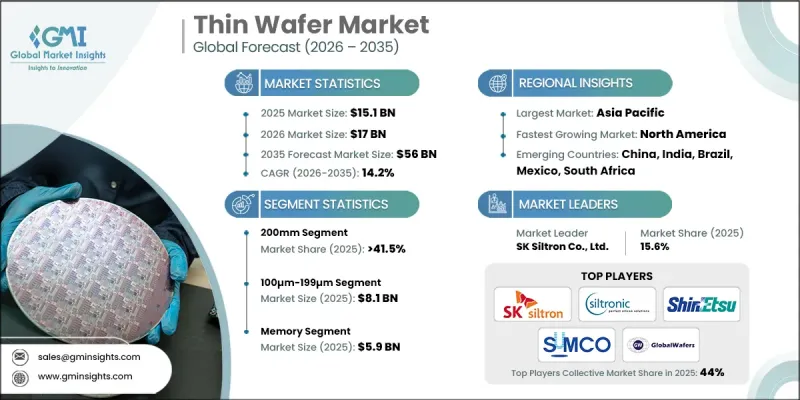
全球薄晶圓市場預計到 2025 年價值 151 億美元,預計到 2035 年將達到 560 億美元,年複合成長率為 14.2%。
超薄晶圓是採用先進的背面研磨、精密拋光和化學蝕刻技術加工而成的半導體基板,其厚度可達200微米或更薄(表面處理後通常為50微米至100微米)。這些超薄基板對於新一代功率元件和緊湊型電子架構至關重要,尤其是在需要高密度整合且總厚度偏差控制在1微米以內的3D堆疊應用中。其結構均勻性最大限度地減少了翹曲,並確保了在先進封裝製程中的可靠操作。對小型電子設備、高效能運算和高效能電源管理解決方案日益成長的需求正在加速超薄晶圓在各行各業的應用。半導體製造技術和材料工程的不斷進步進一步提高了晶圓的耐久性、產量比率和電氣性能,使超薄晶圓成為現代半導體製造的基本組成部分。
| 市場範圍 | |
|---|---|
| 開始年份 | 2025 |
| 預測期 | 2026-2035 |
| 上市時的市場規模 | 151億美元 |
| 預計金額 | 560億美元 |
| 複合年成長率 | 14.2% |
汽車產業電氣化和自動化技術的進步顯著推動了對薄晶圓的需求成長。不斷提高的車輛燃油效率標準和減少排放氣體的努力正在加速先進半導體元件的整合。新興市場電動車的日益普及,以及對充電基礎設施和電子控制技術的投資,正在推動市場擴張。此外,公共和私人對半導體生產投資的增加,以及主要企業之間活性化的研發合作,正在加速技術進步並擴大製造能力。
預計2026年至2035年間,125mm/150mm晶圓尺寸市場將以13.8%的複合年成長率成長。推動這一市場成長的主要因素是汽車產業對緊湊型、高效能功率積體電路和感測器解決方案的需求不斷成長。連網型設備、先進通訊基礎設施和家用電子電器的普及,持續推動成熟節點製造流程的發展,這些製程利用較小的晶圓尺寸來實現更具成本效益的生產。
預計到2025年,厚度為100μm至199μm的薄晶圓市場規模將達到81億美元。由於其在功率半導體應用中的日益普及,尤其是在支援電動車和可再生能源系統方面,該細分市場佔據了最大的市場佔有率。此厚度範圍內的薄晶圓在機械強度和電氣效率之間實現了最佳平衡,從而支援感測器、電源管理積體電路和先進3D封裝架構的大規模生產。製造商正致力於開發先進的瞬態鍵合解決方案和載流子晶圓技術,以提高高功率半導體裝置的製程穩定性和性能。
預計到2025年,北美薄晶圓市場將佔據15.7%的市場。這一區域成長主要得益於汽車平台向電氣化轉型,而電氣化汽車平台則需要更高的半導體負載能力來支援先進的控制和安全系統。醫療設備製造業的擴張、人口結構變化以及對半導體製造的策略性投資,都將推動該地區在2035年之前持續發展。
目錄
第1章:調查方法和範圍
第2章執行摘要
第3章業界考察
- 生態系分析
- 供應商情況
- 利潤率
- 成本結構
- 每個階段增加的價值
- 影響價值鏈的因素
- 中斷
- 影響產業的因素
- 促進因素
- 對先進半導體封裝的需求
- 5G和人工智慧晶片的普及
- 物聯網設備的廣泛應用
- 電動車的電力電子設備
- CMOS影像感測器的發展
- 產業潛在風險與挑戰
- 晶圓翹曲和處理方面的挑戰
- 缺陷密度高,良率產量比率
- 市場機遇
- 先進包裝創新
- 功率半導體領域的轉變
- 促進因素
- 成長潛力分析
- 監理情勢
- 北美洲
- 歐洲
- 亞太地區
- 拉丁美洲
- 中東和非洲
- 波特的分析
- PESTEL 分析
- 科技與創新趨勢
- 當前技術趨勢
- 新興技術
- 價格趨勢
- 歷史價格分析(2022-2024)
- 影響價格趨勢的因素
- 各地區價格波動
- 價格預測(2026-2035)
- 定價策略
- 新興經營模式
- 合規要求
- 專利分析
第4章 競爭情勢
- 介紹
- 企業市佔率分析
- 按地區
- 北美洲
- 歐洲
- 亞太地區
- 拉丁美洲
- 中東和非洲
- 市場集中度分析
- 按地區
- 主要企業的競爭標竿分析
- 財務績效比較
- 銷售量
- 利潤率
- 研究與開發
- 產品系列比較
- 產品線
- 科技
- 創新
- 區域擴張比較
- 全球擴張分析
- 服務網路覆蓋
- 按地區分類的市場滲透率
- 競爭定位矩陣
- 領導者
- 挑戰者
- 追蹤者
- 小眾玩家
- 戰略展望矩陣
- 財務績效比較
- 2022-2025 年重大發展
- 併購
- 夥伴關係和聯盟
- 技術進步
- 業務拓展與投資策略
- 永續發展計劃
- 數位轉型計劃
- 新興/Start-Ups競爭對手的發展趨勢
第5章 市場估計與預測:依厚度分類,2022-2035年
- ,
- 超過 200μm
- 100微米至199微米
- 50微米至99微米
- 30微米至49微米
- 10微米至29微米
- 小於10微米
第6章 依晶圓尺寸分類的市場估算與預測,2022-2035年
- 100 mm
- 125 mm/150 mm
- 200 mm
- 300 mm
第7章 市場估價與預測:依製程分類,2022-2035年
- 暫時黏合剝離
- UV釋放黏合劑
- 黏合劑
- 溶劑釋放黏合劑
- 無載體系統/泰科工藝
第8章 市場估計與預測:依應用領域分類,2022-2035年
- MEMS
- CMOS影像感測器
- 記憶
- 射頻設備
- LED
- 中介
- 邏輯
- 其他
第9章 市場估計與預測:依地區分類,2022-2035年
- 按地區
- 北美洲
- 美國
- 加拿大
- 歐洲
- 英國
- 德國
- 法國
- 義大利
- 西班牙
- 荷蘭
- 其他歐洲地區
- 亞太地區
- 中國
- 印度
- 日本
- 韓國
- 澳洲
- 亞太其他地區
- 拉丁美洲
- 巴西
- 墨西哥
- 阿根廷
- 其他拉丁美洲地區
- 中東和非洲(MEA)
- 沙烏地阿拉伯
- 南非
- 阿拉伯聯合大公國
- 其他中東和非洲地區
第10章:公司簡介
- 3M
- Applied Materials
- Brewer Science
- Disco Corporation
- EV Group
- GlobalWafers Co. Ltd.
- IceMOS Technology Ltd.
- Mechatronic Systemtechnik GmbH
- Okmetic
- Polishing Corporation of America
- Shanghai Simgui Technology Co. Ltd.
- Shin-Etsu Chemical Co., Ltd.
- Silicon Valley Microelectronics, Inc
- Siltronic AG
- Sil'tronix Silicon Technologies
- SK Siltron Co., Ltd.
- Skynova SA
- SOITEC
- SUMCO CORPORATION
- SUSS MicroTec
- UniversityWafer, Inc
- Virginia Semiconductor Inc.
- Wafer Works Corporation
- Wafer World Inc.
- WaferPro
The Global Thin Wafer Market was valued at USD 15.1 billion in 2025 and is estimated to grow at a CAGR of 14.2% to reach USD 56 billion by 2035.
Thin wafers are semiconductor substrates processed through advanced back grinding, precision polishing, and chemical etching techniques to achieve a thickness of 200μm or below, typically ranging between 50μm and 100μm after front-side fabrication. These ultra-thin substrates are critical for next-generation power devices and compact electronic architectures, particularly in 3D stacking applications where high-density integration is required without exceeding 1μm total thickness variation. Their structural uniformity minimizes warping while enabling reliable handling during advanced packaging processes. Rising demand for miniaturized electronics, high-performance computing, and efficient power management solutions is accelerating adoption across multiple industries. Continuous advancements in semiconductor fabrication technologies and material engineering are further enhancing wafer durability, yield rates, and electrical performance, positioning thin wafers as a foundational component in modern semiconductor manufacturing.
| Market Scope | |
|---|---|
| Start Year | 2025 |
| Forecast Year | 2026-2035 |
| Start Value | $15.1 Billion |
| Forecast Value | $56 Billion |
| CAGR | 14.2% |
Growing electrification and automation within the automotive sector are significantly contributing to thin wafer demand. Increasing vehicle efficiency standards and emission reduction initiatives are driving the integration of advanced semiconductor components. Expanding electric vehicle adoption across emerging economies, along with investments in charging infrastructure and electronic control technologies, is reinforcing market expansion. In addition, public and private sector investments in semiconductor production, combined with rising research and development collaboration among leading players, are accelerating technological progress and manufacturing capacity growth.
The 125 mm/150 mm wafer size segment is expected to grow at a CAGR of 13.8% during 2026-2035. Rising automotive demand for compact and high-efficiency power integrated circuits and sensor solutions is fueling this segment. Broader deployment of connected devices, advanced communication infrastructure, and consumer electronics continues to support mature-node production processes utilizing smaller wafer formats for cost-effective manufacturing.
The 100μm-199μm thickness segment generated USD 8.1 billion in 2025. This segment maintains the largest share due to increasing utilization in power semiconductor applications supporting electric mobility and renewable energy systems. Thin wafers within this thickness range provide an optimal balance between mechanical integrity and electrical efficiency, supporting high-volume sensor manufacturing, power management integrated circuits, and advanced 3D packaging architectures. Manufacturers are emphasizing sophisticated temporary bonding solutions and carrier wafer technologies to improve process stability and performance outcomes in high-power semiconductor devices.
North America Thin Wafer Market accounted for 15.7% share in 2025. Regional growth is supported by the transition toward electrified automotive platforms, which require increased semiconductor content for advanced control and safety systems. Expansion in medical device manufacturing, demographic trends, and strategic semiconductor fabrication investments are contributing to sustained regional development through 2035.
Prominent companies operating in the Global Thin Wafer Market include SUMCO CORPORATION, Shin-Etsu Chemical Co., Ltd., Siltronic AG, GlobalWafers Co. Ltd., SK Siltron Co., Ltd., SOITEC, Applied Materials, Disco Corporation, EV Group, SUSS MicroTec, Okmetic, 3M, Brewer Science, Silicon Valley Microelectronics, Inc., UniversityWafer, Inc., Virginia Semiconductor Inc., Wafer Works Corporation, Shanghai Simgui Technology Co. Ltd., IceMOS Technology Ltd., Mechatronic Systemtechnik GmbH, Polishing Corporation of America, Sil'tronix Silicon Technologies, Skynova SA, Wafer World Inc., and WaferPro. Companies in the Global Thin Wafer Market are strengthening their competitive position through technological innovation, strategic alliances, and capacity expansion. Manufacturers are investing heavily in advanced material processing techniques, precision thinning equipment, and bonding technologies to enhance wafer uniformity and yield performance. Strategic collaborations with semiconductor foundries and device manufacturers enable early integration into next-generation chip designs. Firms are also expanding fabrication facilities to address rising global demand and improve supply chain resilience. Portfolio diversification into specialty substrates and engineered wafer solutions supports broader customer engagement.
Table of Contents
Chapter 1 Methodology and Scope
- 1.1 Market scope and definition
- 1.2 Research design
- 1.2.1 Research approach
- 1.2.2 Data collection methods
- 1.3 Data mining sources
- 1.3.1 Global
- 1.3.2 Regional/Country
- 1.4 Base estimates and calculations
- 1.4.1 Base year calculation
- 1.4.2 Key trends for market estimation
- 1.5 Primary research and validation
- 1.5.1 Primary sources
- 1.6 Forecast model
- 1.7 Research assumptions and limitations
Chapter 2 Executive Summary
- 2.1 Industry snapshot
- 2.2 Key market trends
- 2.2.1 Thickness trends
- 2.2.2 Wafer size trends
- 2.2.3 Process trends
- 2.2.4 Application trends
- 2.2.5 Regional trends
- 2.3 TAM Analysis, 2025-2034 (USD Billion)
- 2.4 CXO perspectives: Strategic imperatives
- 2.4.1 Executive decision points
- 2.4.2 critical success factors
- 2.5 Future outlook and strategic recommendations
Chapter 3 Industry Insights
- 3.1 Industry ecosystem analysis
- 3.1.1 Supplier Landscape
- 3.1.2 Profit Margin
- 3.1.3 Cost structure
- 3.1.4 Value addition at each stage
- 3.1.5 Factor affecting the value chain
- 3.1.6 Disruptions
- 3.2 Industry impact forces
- 3.2.1 Growth drivers
- 3.2.1.1 Advanced Semiconductor Packaging Demand
- 3.2.1.2 5G and AI Chip Proliferation
- 3.2.1.3 IoT Device Expansion
- 3.2.1.4 Electric Vehicle Power Electronics
- 3.2.1.5 CMOS Image Sensor Growth
- 3.2.2 Industry pitfalls and challenges
- 3.2.2.1 Wafer Warpage and Handling Challenges
- 3.2.2.2 High Defect Density and Yield Loss
- 3.2.3 Market opportunities
- 3.2.3.1 Advanced Packaging Innovation
- 3.2.3.2 Power Semiconductor Shift
- 3.2.1 Growth drivers
- 3.3 Growth potential analysis
- 3.4 Regulatory landscape
- 3.4.1 North America
- 3.4.2 Europe
- 3.4.3 Asia Pacific
- 3.4.4 Latin America
- 3.4.5 Middle East & Africa
- 3.5 Porter’s analysis
- 3.6 PESTEL analysis
- 3.7 Technology and innovation landscape
- 3.7.1 Current technological trends
- 3.7.2 Emerging technologies
- 3.8 Price trends
- 3.8.1 Historical price analysis (2022-2024)
- 3.8.2 Price trend drivers
- 3.8.3 Regional price variations
- 3.8.4 Price forecast (2026-2035)
- 3.9 Pricing strategies
- 3.10 Emerging business models
- 3.11 Compliance requirements
- 3.12 Patent analysis
Chapter 4 Competitive Landscape, 2025
- 4.1 Introduction
- 4.2 Company market share analysis
- 4.2.1 By Region
- 4.2.1.1 North America
- 4.2.1.2 Europe
- 4.2.1.3 Asia Pacific
- 4.2.1.4 Latin America
- 4.2.1.5 Middle East & Africa
- 4.2.2 Market Concentration Analysis
- 4.2.1 By Region
- 4.3 Competitive benchmarking of key players
- 4.3.1 Financial performance comparison
- 4.3.1.1 Revenue
- 4.3.1.2 Profit margin
- 4.3.1.3 R&D
- 4.3.2 Product portfolio comparison
- 4.3.2.1 Product range breadth
- 4.3.2.2 Technology
- 4.3.2.3 Innovation
- 4.3.3 Geographic presence comparison
- 4.3.3.1 Global footprint analysis
- 4.3.3.2 Service network coverage
- 4.3.3.3 Market penetration by region
- 4.3.4 Competitive positioning matrix
- 4.3.4.1 Leaders
- 4.3.4.2 Challengers
- 4.3.4.3 Followers
- 4.3.4.4 Niche players
- 4.3.5 Strategic outlook matrix
- 4.3.1 Financial performance comparison
- 4.4 Key developments, 2022-2025
- 4.4.1 Mergers and acquisitions
- 4.4.2 Partnerships and collaborations
- 4.4.3 Technological advancements
- 4.4.4 Expansion and investment strategies
- 4.4.5 Sustainability initiatives
- 4.4.6 Digital transformation initiatives
- 4.5 Emerging/ startup competitors landscape
Chapter 5 Market Estimates & Forecast, By Thickness, 2022 - 2035 (USD Million)
- 5.1 Key trends,
- 5.2 >200μm
- 5.3 100μm-199μm
- 5.4 50μm-99μm
- 5.5 30μm-49μm
- 5.6 10μm-29μm
- 5.7 <10μm
Chapter 6 Market Estimates and Forecast, By Wafer Size, 2022 - 2035 (USD Million)
- 6.1 Key trends
- 6.2 100 mm
- 6.3 125 mm/150mm
- 6.4 200 mm
- 6.5 300 mm
Chapter 7 Market Estimates and Forecast, By Process, 2022 - 2035 (USD Million)
- 7.1 Key trends
- 7.2 Temporary bonding & debonding
- 7.2.1 UV-release adhesives
- 7.2.2 Thermal-release adhesives
- 7.2.3 Solvent-release adhesives
- 7.3 Carrier-less approach/Taiko process
Chapter 8 Market Estimates and Forecast, By Application, 2022 - 2035 (USD Million)
- 8.1 Key trends
- 8.2 MEMS
- 8.3 CMOS image sensors
- 8.4 Memory
- 8.5 RF devices
- 8.6 LED
- 8.7 Interposers
- 8.8 Logic
- 8.9 Others
Chapter 9 Market Estimates & Forecast, By Region, 2022 - 2035 (USD Million)
- 9.1 Key trends, by region
- 9.2 North America
- 9.2.1 U.S.
- 9.2.2 Canada
- 9.3 Europe
- 9.3.1 UK
- 9.3.2 Germany
- 9.3.3 France
- 9.3.4 Italy
- 9.3.5 Spain
- 9.3.6 Netherlands
- 9.3.7 Rest of Europe
- 9.4 Asia-Pacific
- 9.4.1 China
- 9.4.2 India
- 9.4.3 Japan
- 9.4.4 South Korea
- 9.4.5 Australia
- 9.4.6 Rest of Asia-Pacific
- 9.5 Latin America
- 9.5.1 Brazil
- 9.5.2 Mexico
- 9.5.3 Argentina
- 9.5.4 Rest of Latin America
- 9.6 MEA
- 9.6.1 Saudi Arabia
- 9.6.2 South Africa
- 9.6.3 UAE
- 9.6.4 Rest of MEA
Chapter 10 Company Profiles
- 10.1 3M
- 10.2 Applied Materials
- 10.3 Brewer Science
- 10.4 Disco Corporation
- 10.5 EV Group
- 10.6 GlobalWafers Co. Ltd.
- 10.7 IceMOS Technology Ltd.
- 10.8 Mechatronic Systemtechnik GmbH
- 10.9 Okmetic
- 10.10 Polishing Corporation of America
- 10.11 Shanghai Simgui Technology Co. Ltd.
- 10.12 Shin-Etsu Chemical Co., Ltd.
- 10.13 Silicon Valley Microelectronics, Inc
- 10.14 Siltronic AG
- 10.15 Sil'tronix Silicon Technologies
- 10.16 SK Siltron Co., Ltd.
- 10.17 Skynova SA
- 10.18 SOITEC
- 10.19 SUMCO CORPORATION
- 10.20 SUSS MicroTec
- 10.21 UniversityWafer, Inc
- 10.22 Virginia Semiconductor Inc.
- 10.23 Wafer Works Corporation
- 10.24 Wafer World Inc.
- 10.25 WaferPro
 薄晶圓市場:依材料、晶圓尺寸、製造流程、應用和最終用途產業分類-2026-2032年全球市場預測
 全球薄晶圓市場規模、佔有率、趨勢和成長分析報告(2026-2034)薄晶圓FOSB市場:依晶圓直徑、材料類型、厚度範圍、表面處理、應用、終端用戶產業和分銷管道分類-全球預測,2026-2032年薄晶圓FOUP市場:2026年至2032年全球預測(依晶圓尺寸、產品類型、產能、材質、自動化程度、最終用戶和應用分類)
 全球薄晶圓市場:依厚度、應用、材料、終端用戶產業、國家及地區分類-產業分析、市場規模、佔有率及未來預測(2025-2032年)
 2026年全球薄晶圓市場報告
 2026-2030年全球磷化銦(InP)晶圓市場薄晶圓市場-2025年至2030年的預測