

 |
市場調查報告書
商品編碼
1959280
先進半導體封裝市場機會、成長要素、產業趨勢分析及2026年至2035年預測Advanced Semiconductor Packaging Market Opportunity, Growth Drivers, Industry Trend Analysis, and Forecast 2026 - 2035 |
||||||
2025年全球先進半導體封裝市場價值為335億美元,預計2035年將達953億美元,年複合成長率為11%。
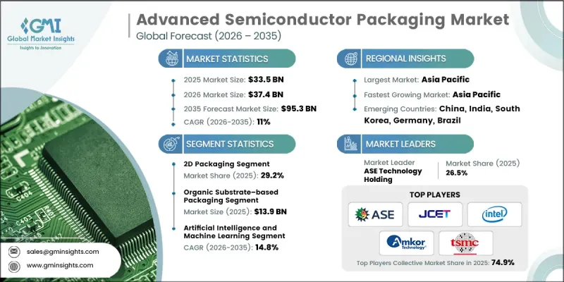
市場擴張的驅動力主要來自晶片級處理器架構的加速發展以及下一代無線基礎設施的廣泛部署。這些趨勢正在加速對高密度射頻整合技術和系統級封裝)配置的需求,以支援緊湊型高性能電子設備。同時,先進製程節點不斷上漲的製造成本和產量比率,使得業界更加重視先進封裝技術,將其視為提升效能和成本效益的關鍵促進因素。此外,人工智慧加速器日益普及,需要高頻寬記憶體整合,這也進一步推動了市場需求,因為這些配置能夠實現高吞吐量,滿足高要求的運算工作負載的需求。同時,超大規模資料中心和高效能運算平台的擴展也推動了2.5D和3D積體電路架構的應用。這些封裝創新實現了異質整合、更高的互連密度和更強的能源效率,進一步提升了它們在下一代半導體設計中的戰略重要性。
| 市場範圍 | |
|---|---|
| 開始年份 | 2025 |
| 預測年份 | 2026-2035 |
| 起始值 | 335億美元 |
| 預測金額 | 953億美元 |
| 複合年成長率 | 11% |
2025年,2D封裝仍維持其最大市場佔有率,達29.2%。其持續領先地位得益於成熟邏輯節點、類比元件、電源管理元件和混合訊號積體電路的高使用率。由於成本穩定、製造可靠性高且產量比率最佳化,這種封裝形式對大規模生產仍然極具吸引力。家用電子電器、汽車系統和工業自動化等關鍵終端用戶產業繼續依賴2D封裝,以實現與現有製造流程和穩健供應鏈的無縫整合。其擴充性和久經考驗的可靠性確保了在大批量生產環境中的持續需求。
預計到2025年,基於有機基板的封裝市場規模將達到139億美元。該領域的成長主要得益於覆晶封裝和先進多層封裝設計在處理器、連接組件和汽車電子產品中的廣泛應用。有機基板兼具優異的電氣性能、機械柔軟性和成本效益,使其成為高輸入/輸出密度應用的理想選擇。成熟的生產生態系統和持續的材料創新進一步推動了該領域的成長。在消費性電子設備、通訊基礎設施和工業系統等領域,對性能穩定性和大規模生產能力的需求仍然強勁。
預計到2025年,北美先進半導體封裝市場佔有率將達到22.8%。在人工智慧處理器和先進資料中心晶片需求不斷成長的推動下,該地區的發展正在加速。由整合裝置製造商和外包半導體組裝測試服務商組成的強大生態系統,為先進封裝技術的快速普及提供了有力支援。 2.5D和3D整合策略的日益普及,使區域內企業能夠克服傳統平面架構在效能、頻寬和功耗方面的限制。對半導體研發、本土製造能力和先進運算基礎設施的持續投入,進一步鞏固了北美在全球市場的競爭優勢。
目錄
第1章:調查方法和範圍
第2章執行摘要
第3章業界考察
- 生態系分析
- 供應商情況
- 利潤率
- 成本結構
- 每個階段增加的價值
- 影響價值鏈的因素
- 中斷
- 影響產業的因素
- 促進因素
- 需要高頻寬記憶體整合的AI加速器
- 高效能運算和資料中心採用 2.5D 和 3D 積體電路
- Chiplet架構取代了單晶片SoC設計
- 需要高密度射頻封裝的5G基地台
- 先進節點的成本推高了封裝創新的價值。
- 產業潛在風險與挑戰
- 對先進包裝工廠的高資本投入
- 高功率封裝元件溫度控管的複雜性
- 市場機遇
- 透過代工廠與OSAT廠商的夥伴關係,擴大先進封裝產能。
- 用於下一代資料中心互連的聯合封裝光元件
- 促進因素
- 成長潛力分析
- 監理情勢
- 波特五力分析
- PESTEL 分析
- 科技與創新趨勢
- 當前技術趨勢
- 新興技術
- 價格趨勢
- 按地區
- 依產品
- 定價策略
- 新興經營模式
- 合規要求
- 專利和智慧財產權分析
- 地緣政治和貿易趨勢
第4章 競爭情勢
- 介紹
- 企業市佔率分析
- 按地區
- 市場集中度分析
- 主要企業的競爭標竿分析
- 財務績效比較
- 收入
- 利潤率
- 研究與開發
- 產品系列比較
- 產品線廣度
- 科技
- 創新
- 地理位置比較
- 全球擴張分析
- 服務網路覆蓋
- 按地區分類的市場滲透率
- 競爭定位矩陣
- 領導企業
- 受讓人
- 追蹤者
- 小眾玩家
- 戰略展望矩陣
- 財務績效比較
- 主要進展
- 併購
- 夥伴關係與合作
- 技術進步
- 擴張和投資策略
- 數位轉型計劃
- 新興/Start-Ups競爭對手的發展趨勢
第5章 市場估價與預測:依包裝架構分類,2022-2035年
- 2D封裝(單晶粒,單平面)
- 2.5D封裝(多晶片、基於中介層的單垂直平面)
- 3D封裝(垂直晶粒堆疊)
- 基於TSV的3D封裝
- 基於混合鍵結的3D包裝
- 晶圓層次電子構裝(WLP)
- 扇入晶圓層次電子構裝(FI-WLP)
- 扇出型晶圓層次電子構裝(FO-WLP)
- 混合/多架構封裝
第6章 市場估價與預測:依包裝材料分類,2022-2035年
- 基於有機基板的包裝
- 基於矽中介層的封裝
- 基於RDL(重構晶圓)的封裝
- 3D堆疊是主流封裝方法(晶粒間連接材料平台)。
- 基於玻璃中介層的封裝
第7章 市場估計與預測:依應用領域分類,2022-2035年
- 人工智慧和機器學習
- 高效能運算 (HPC) 和資料中心
- 行動通訊
- 車
- 家用電子電器
- 工業、航太和國防領域。
第8章 市場估計與預測:依地區分類,2022-2035年
- 北美洲
- 美國
- 加拿大
- 歐洲
- 德國
- 英國
- 法國
- 西班牙
- 義大利
- 俄羅斯
- 亞太地區
- 中國
- 印度
- 日本
- 澳洲
- 韓國
- 拉丁美洲
- 巴西
- 墨西哥
- 阿根廷
- 中東和非洲
- 南非
- 沙烏地阿拉伯
- 阿拉伯聯合大公國
第9章:公司簡介
- 主要企業
- ASE Technology Holding
- Amkor Technology, Inc.
- Taiwan Semiconductor Manufacturing Company(TSMC)
- Samsung Electronics
- Intel Corporation
- 按地區分類的主要企業
- 北美洲
- GlobalFoundries Inc.
- Texas Instruments
- Micron Technology, Inc.
- 亞太地區
- JCET Group Co., Ltd.
- Powertech Technology Inc.(PTI)
- Huatian Technology Co., Ltd.
- Tongfu Microelectronics Co., Ltd.
- ChipMOS Technologies Inc.
- UTAC Holdings Ltd.
- HANA Micron Inc.
- SK hynix
- 北美洲
- 特殊玩家/干擾者
- China Wafer Level CSP Co., Ltd.(CWLP)
The Global Advanced Semiconductor Packaging Market was valued at USD 33.5 billion in 2025 and is estimated to grow at a CAGR of 11% to reach USD 95.3 billion by 2035.
Market expansion is fueled by the increasing transition toward chiplet-based processor architectures and the widespread deployment of next-generation wireless infrastructure. These trends are accelerating demand for high-density radio frequency integration and system-in-package configurations that support compact, high-performance electronics. At the same time, escalating fabrication costs and yield constraints at leading-edge process nodes are shifting industry focus toward advanced packaging as a critical driver of performance gains and cost efficiency. The growing adoption of AI accelerators that require high-bandwidth memory integration is further strengthening demand, as these configurations enable extremely high data throughput essential for advanced computing workloads. In addition, expansion of hyperscale data centers and high-performance computing platforms is driving the implementation of 2.5D and 3D integrated circuit architectures. These packaging innovations enable heterogeneous integration, improved interconnect density, and enhanced power efficiency, reinforcing their strategic importance in next-generation semiconductor design.
| Market Scope | |
|---|---|
| Start Year | 2025 |
| Forecast Year | 2026-2035 |
| Start Value | $33.5 Billion |
| Forecast Value | $95.3 Billion |
| CAGR | 11% |
In 2025, the 2D packaging segment accounted for 29.2% share, maintaining the largest share. Its continued dominance is supported by strong utilization across mature logic nodes, analog components, power management devices, and mixed-signal integrated circuits. This packaging format remains highly attractive for large-scale production due to its cost stability, manufacturing reliability, and optimized yield performance. Key end-use industries, including consumer electronics, automotive systems, and industrial automation, continue to depend on 2D packaging because it aligns seamlessly with established fabrication processes and resilient supply networks. Its scalability and proven reliability ensure consistent demand across high-volume production environments.
The organic substrate-based packaging segment reached USD 13.9 billion in 2025. Growth in this category is driven by widespread deployment in flip-chip assemblies and advanced laminate package designs used in processors, connectivity components, and automotive electronics. Organic substrates provide an optimal combination of electrical performance, mechanical flexibility, and cost efficiency, making them well-suited for applications requiring high input/output density. Established production ecosystems and continuous material innovation further reinforce segment growth. Demand remains strong across consumer devices, communications infrastructure, and industrial systems, where performance consistency and manufacturability at scale are essential.
North America Advanced Semiconductor Packaging Market held a 22.8% share in 2025. The region is experiencing accelerated development driven by rising demand for AI-enabled processors and advanced data center chips. A robust ecosystem of integrated device manufacturers and outsourced semiconductor assembly and test providers supports rapid adoption of advanced packaging technologies. Increasing implementation of 2.5D and 3D integration strategies is helping regional players overcome performance, bandwidth, and power limitations associated with conventional planar architectures. Continued investment in semiconductor research, domestic manufacturing capabilities, and advanced computing infrastructure is further strengthening North America's competitive position in the global market.
Key companies operating in the Global Advanced Semiconductor Packaging Market include Taiwan Semiconductor Manufacturing Company (TSMC), Samsung Electronics, Intel Corporation, Amkor Technology, Inc., ASE Technology Holding, JCET Group Co., Ltd., Powertech Technology Inc. (PTI), GlobalFoundries Inc., Micron Technology, Inc., SK hynix, Texas Instruments, Tongfu Microelectronics Co., Ltd., Huatian Technology Co., Ltd., ChipMOS Technologies Inc., HANA Micron Inc., China Wafer Level CSP Co., Ltd. (CWLP), and UTAC Holdings Ltd. Companies in the Advanced Semiconductor Packaging Market are reinforcing their market position through strategic investments in research and development focused on high-density interconnect technologies and advanced substrate materials. Many players are expanding manufacturing capacity to meet rising demand from AI, high-performance computing, and automotive electronics sectors. Collaborative partnerships with foundries, memory manufacturers, and system designers are enabling co-optimization of chip architecture and packaging solutions. Firms are also prioritizing vertical integration to improve supply chain resilience and reduce production bottlenecks.
Table of Contents
Chapter 1 Methodology and Scope
- 1.1 Market scope and definition
- 1.2 Research design
- 1.2.1 Research approach
- 1.2.2 Data collection methods
- 1.3 Data mining sources
- 1.3.1 Global
- 1.3.2 Regional/Country
- 1.4 Base estimates and calculations
- 1.4.1 Base year calculation
- 1.4.2 Key trends for market estimation
- 1.5 Primary research and validation
- 1.5.1 Primary sources
- 1.6 Forecast model
- 1.7 Research assumptions and limitations
Chapter 2 Executive Summary
- 2.1 Industry 360° synopsis, 2022 - 2035
- 2.2 Key market trends
- 2.2.1 Packaging architecture trends
- 2.2.2 Packaging material trends
- 2.2.3 Application trends
- 2.2.4 Regional trends
- 2.3 TAM Analysis, 2026-2035
- 2.4 CXO perspectives: Strategic imperatives
- 2.4.1 Executive decision points
- 2.4.2 critical success factors
- 2.5 Future outlook and strategic recommendations
Chapter 3 Industry Insights
- 3.1 Industry ecosystem analysis
- 3.1.1 Supplier Landscape
- 3.1.2 Profit Margin
- 3.1.3 Cost structure
- 3.1.4 Value addition at each stage
- 3.1.5 Factor affecting the value chain
- 3.1.6 Disruptions
- 3.2 Industry impact forces
- 3.2.1 Growth drivers
- 3.2.1.1 AI accelerators demanding high-bandwidth memory integration
- 3.2.1.2 HPC and data centers adopting 2.5D and 3D ICs
- 3.2.1.3 Chiplet architectures replacing monolithic SoC designs
- 3.2.1.4 5G base stations requiring high-density RF packaging
- 3.2.1.5 Advanced nodes cost pushing value toward packaging innovation
- 3.2.2 Industry pitfalls and challenges
- 3.2.2.1 High capital expenditure for advanced packaging fabs
- 3.2.2.2 Thermal management complexity in high-power packaged devices
- 3.2.3 Market opportunities
- 3.2.3.1 Foundry-OSAT partnerships for advanced packaging capacity expansion
- 3.2.3.2 Co-packaged optics enabling next-generation data center interconnects
- 3.2.1 Growth drivers
- 3.3 Growth potential analysis
- 3.4 Regulatory landscape
- 3.4.1 North America
- 3.4.2 Europe
- 3.4.3 Asia Pacific
- 3.4.4 Latin America
- 3.4.5 Middle East & Africa
- 3.5 Porter's analysis
- 3.6 PESTEL analysis
- 3.7 Technology and Innovation landscape
- 3.7.1 Current technological trends
- 3.7.2 Emerging technologies
- 3.8 Price trends
- 3.8.1 By region
- 3.8.2 By product
- 3.9 Pricing Strategies
- 3.10 Emerging Business Models
- 3.11 Compliance Requirements
- 3.12 Patent and IP analysis
- 3.13 Geopolitical and trade dynamics
Chapter 4 Competitive Landscape, 2025
- 4.1 Introduction
- 4.2 Company market share analysis
- 4.2.1 By region
- 4.2.1.1 North America
- 4.2.1.2 Europe
- 4.2.1.3 Asia Pacific
- 4.2.1.4 Latin America
- 4.2.1.5 Middle East & Africa
- 4.2.2 Market concentration analysis
- 4.2.1 By region
- 4.3 Competitive benchmarking of key players
- 4.3.1 Financial performance comparison
- 4.3.1.1 Revenue
- 4.3.1.2 Profit margin
- 4.3.1.3 R&D
- 4.3.2 Product portfolio comparison
- 4.3.2.1 Product range breadth
- 4.3.2.2 Technology
- 4.3.2.3 Innovation
- 4.3.3 Geographic presence comparison
- 4.3.3.1 Global footprint analysis
- 4.3.3.2 Service network coverage
- 4.3.3.3 Market penetration by region
- 4.3.4 Competitive positioning matrix
- 4.3.4.1 Leaders
- 4.3.4.2 Challengers
- 4.3.4.3 Followers
- 4.3.4.4 Niche players
- 4.3.5 Strategic outlook matrix
- 4.3.1 Financial performance comparison
- 4.4 Key developments
- 4.4.1 Mergers and acquisitions
- 4.4.2 Partnerships and collaborations
- 4.4.3 Technological advancements
- 4.4.4 Expansion and investment strategies
- 4.4.5 Digital transformation initiatives
- 4.5 Emerging/ startup competitors landscape
Chapter 5 Market Estimates and Forecast, By Packaging Architecture, 2022 - 2035 (USD Million)
- 5.1 Key trends
- 5.2 2D Packaging (single-die, single-plane)
- 5.3 2.5D Packaging (multi-die, interposer-based, single vertical plane)
- 5.4 3D Packaging (Vertical Die Stacking)
- 5.4.1 TSV-based 3D packaging
- 5.4.2 Hybrid bonding-based 3D packaging
- 5.5 Wafer-level packaging (WLP)
- 5.5.1 Fan-in wafer-level packaging (FI-WLP)
- 5.5.2 Fan-out wafer-level packaging (FO-WLP)
- 5.6 Hybrid/multi-architecture packaging
Chapter 6 Market Estimates and Forecast, By Packaging Material, 2022 - 2035 (USD Million)
- 6.1 Key trends
- 6.2 Organic substrate-based packaging
- 6.3 Silicon interposer-based packaging
- 6.4 RDL-based (reconstituted wafer) packaging
- 6.5 3D stack-dominant packaging (die-to-die material platform)
- 6.6 Glass interposer-based packaging
Chapter 7 Market Estimates and Forecast, By Application, 2022 - 2035 (USD Million)
- 7.1 Key trends
- 7.2 Artificial intelligence and machine learning
- 7.3 High-performance computing (HPC) and data center
- 7.4 Mobile and communications
- 7.5 Automotive
- 7.6 Consumer electronics
- 7.7 Industrial, aerospace and defense
Chapter 8 Market Estimates and Forecast, By Region, 2022 - 2035 (USD Million)
- 8.1 Key trends
- 8.2 North America
- 8.2.1 U.S.
- 8.2.2 Canada
- 8.3 Europe
- 8.3.1 Germany
- 8.3.2 UK
- 8.3.3 France
- 8.3.4 Spain
- 8.3.5 Italy
- 8.3.6 Russia
- 8.4 Asia Pacific
- 8.4.1 China
- 8.4.2 India
- 8.4.3 Japan
- 8.4.4 Australia
- 8.4.5 South Korea
- 8.5 Latin America
- 8.5.1 Brazil
- 8.5.2 Mexico
- 8.5.3 Argentina
- 8.6 Middle East and Africa
- 8.6.1 South Africa
- 8.6.2 Saudi Arabia
- 8.6.3 UAE
Chapter 9 Company Profiles
- 9.1 Global Key Players
- 9.1.1 ASE Technology Holding
- 9.1.2 Amkor Technology, Inc.
- 9.1.3 Taiwan Semiconductor Manufacturing Company (TSMC)
- 9.1.4 Samsung Electronics
- 9.1.5 Intel Corporation
- 9.2 Regional key players
- 9.2.1 North America
- 9.2.1.1 GlobalFoundries Inc.
- 9.2.1.2 Texas Instruments
- 9.2.1.3 Micron Technology, Inc.
- 9.2.2 Asia Pacific
- 9.2.2.1 JCET Group Co., Ltd.
- 9.2.2.2 Powertech Technology Inc. (PTI)
- 9.2.2.3 Huatian Technology Co., Ltd.
- 9.2.2.4 Tongfu Microelectronics Co., Ltd.
- 9.2.2.5 ChipMOS Technologies Inc.
- 9.2.2.6 UTAC Holdings Ltd.
- 9.2.2.7 HANA Micron Inc.
- 9.2.2.8 SK hynix
- 9.2.1 North America
- 9.3 Niche Players/Disruptors
- 9.3.1 China Wafer Level CSP Co., Ltd. (CWLP)
 半導體先進封裝市場預測至2034年-按封裝類型、材料、應用、最終用戶和地區分類的全球分析
 2026-2030年全球先進半導體封裝市場
 晶片封裝及測試技術市場:依封裝技術、測試類型、最終用戶、國家及地區分類-全球產業分析、市場規模、市場佔有率及2026年至2033年預測
 全球食品飲料先進包裝市場:依材料類型、包裝形式、類型、應用和地區分類-預測至2031年先進封裝和晶片設計市場預測至2034年-按封裝技術、晶片整合方法、應用、最終用戶和地區分類的全球分析晶片封裝市場預測至2034年-全球分析(依封裝技術、互連技術、晶片類型、材料類型、應用、最終使用者和地區分類)
 先進半導體封裝市場:2026-2032年全球市場預測(依封裝技術、組件、佈線方式、材料類型、間距、最終用途產業及客戶類型分類)
 先進半導體封裝市場分析及預測(至2035年):依類型、產品類型、服務、技術、組件、應用、材料類型、裝置、製程分類先進半導體封裝市場預測至2034年:按封裝類型、材料、製程、互連技術、最終用戶和地區分類的全球分析先進半導體封裝市場,按封裝類型、封裝材料、製造方法、最終用戶、國家和地區分類 - 2025 年至 2032 年全球產業分析、市場規模、市場佔有率及預測