


 |
市場調查報告書
商品編碼
1892717
原子層蝕刻(ALE)設備市場機會、成長促進因素、產業趨勢分析及預測(2025-2034年)Atomic Layer Etching (ALE) Equipment Market Opportunity, Growth Drivers, Industry Trend Analysis, and Forecast 2025 - 2034 |
||||||
2024 年全球原子層蝕刻設備市場價值為 11 億美元,預計到 2034 年將以 8.5% 的複合年成長率成長至 25 億美元。
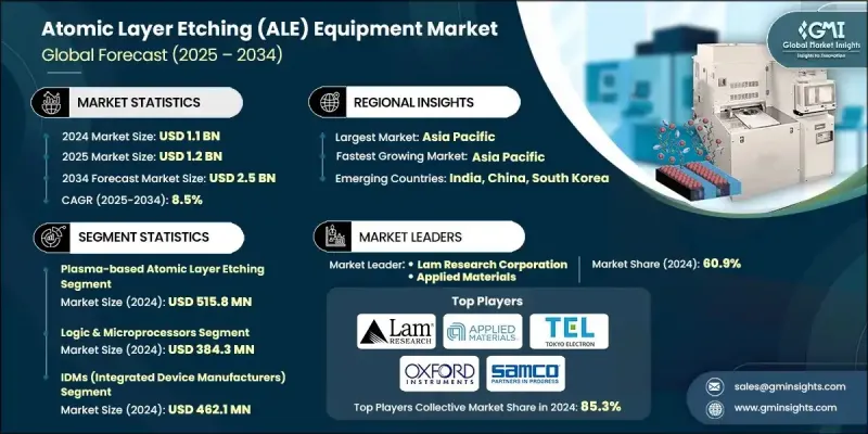
推動成長的因素包括:對緊湊型、高性能半導體元件日益成長的需求、量子技術的快速發展以及對節能電子產品的需求。此外,各公司也積極回應新材料的應用以及裝置小型化趨勢,而這需要具備原子級精度的蝕刻能力。隨著下一代晶片的複雜性不斷提升,業界正大力轉向能夠支援複雜架構的先進工具。量子研究帶來的發展動能也進一步推動了對高精度蝕刻技術的需求,這些技術有助於改進極度敏感元件的製造。
| 市場範圍 | |
|---|---|
| 起始年份 | 2024 |
| 預測年份 | 2025-2034 |
| 起始值 | 11億美元 |
| 預測值 | 25億美元 |
| 複合年成長率 | 8.5% |
2024 年,基於等離子體的原子層蝕刻市場規模達到 5.158 億美元。微電子產業的持續擴張促使供應商增強等離子體原子層蝕刻產品組合,以提供更高的精度、更好的蝕刻選擇性和更嚴格的材料控制,從而滿足先進製造環境中不斷成長的生產需求。
2025年至2034年間,先進封裝元件市場將以11.4%的複合年成長率成長。其成長主要得益於不斷提升的性能需求、5G連接的普及以及在不重新設計核心裝置的情況下整合更多功能的需求。為了滿足現代電子系統不斷變化的封裝需求,各公司正優先推動熱效率、小型化和高密度互連技術的創新。
2024年,美國原子層蝕刻設備市場規模預計將達2.002億美元。這一成長主要得益於聯邦政府對半導體產能的資助、人工智慧和物聯網的蓬勃發展、先進製造流程的進步以及國防應用領域需求的激增。在該地區營運的企業正積極利用投資激勵措施,強化下一代工藝能力,並滿足航太和國防客戶的複雜需求。
目錄
第1章:方法論與範圍
第2章:執行概要
第3章:行業洞察
- 產業生態系分析
- 供應商格局
- 利潤率
- 成本結構
- 每個階段的價值增加
- 影響價值鏈的因素
- 中斷
- 產業生態系分析
- 產業影響因素
- 成長促進因素
- 對更小、更強大的半導體裝置的需求日益成長
- 量子計算的進展
- 對高性能和節能電子產品的需求日益成長
- 先進電子元件新材料的湧現
- 對小型化和複雜積體電路的需求不斷成長
- 陷阱與挑戰
- ALE設備成本高昂
- 與現有製造流程整合的複雜性
- 市場機遇
- 對先進半導體技術的需求不斷成長
- 物聯網和人工智慧新興應用的成長
- 成長促進因素
- 成長潛力分析
- 監管環境
- 北美洲
- 歐洲
- 亞太地區
- 拉丁美洲
- 中東和非洲
- 波特的分析
- PESTEL 分析
- 技術與創新格局
- 當前技術趨勢
- 新興技術
- 價格趨勢
- 按地區
- 依產品
- 定價策略
- 新興商業模式
- 合規要求
- 永續性措施
- 消費者情緒分析
- 專利和智慧財產權分析
- 地緣政治與貿易動態
第4章:競爭格局
- 介紹
- 公司市佔率分析
- 按地區
- 北美洲
- 歐洲
- 亞太地區
- 拉丁美洲
- 中東和非洲
- 市場集中度分析
- 按地區
- 對主要參與者進行競爭基準分析
- 財務績效比較
- 收入
- 利潤率
- 研發
- 產品組合比較
- 產品範圍廣度
- 科技
- 創新
- 地理位置比較
- 全球足跡分析
- 服務網路覆蓋
- 按地區分類的市場滲透率
- 競爭定位矩陣
- 領導人
- 挑戰者
- 追蹤者
- 小眾玩家
- 戰略展望矩陣
- 財務績效比較
- 2021-2024 年主要發展動態
- 併購
- 夥伴關係與合作
- 技術進步
- 擴張和投資策略
- 永續發展舉措
- 數位轉型計劃
- 新興/新創企業競爭對手格局
第5章:市場估計與預測:依技術分類,2021-2034年
- 基於等離子體的原子層蝕刻
- 離子束原子層蝕刻
- 熱原子層蝕刻
- 混合原子層蝕刻
- 其他
第6章:市場估算與預測:依應用領域分類,2021-2034年
- 邏輯與微處理器
- 儲存裝置
- 功率和射頻元件
- 先進包裝
- 光電子學與光子學
- MEMS和感測器
- 其他
第7章:市場估算與預測:依晶圓尺寸分類,2021-2034年
- 200毫米
- 300毫米
- 450毫米
第8章:市場估算與預測:依最終用途分類,2021-2034年
- IDM(整合設備製造商)
- 鑄造廠
- 記憶體製造商
- OSAT/包裝廠
- 其他
第9章:市場估計與預測:依地區分類,2021-2034年
- 北美洲
- 美國
- 加拿大
- 歐洲
- 德國
- 英國
- 法國
- 西班牙
- 義大利
- 荷蘭
- 亞太地區
- 中國
- 印度
- 日本
- 澳洲
- 韓國
- 拉丁美洲
- 巴西
- 墨西哥
- 阿根廷
- 中東和非洲
- 沙烏地阿拉伯
- 南非
- 阿拉伯聯合大公國
第10章:公司簡介
- 全球關鍵參與者
- Lam Research Corporation
- Applied Materials
- Tokyo Electron
- Hitachi High Tech Corporation
- 區域關鍵參與者
- 北美洲
- Mattson Technology, Inc.
- Plasma-Therm
- 歐洲
- Oxford Instruments
- Asia-Pacific
- Samco Inc.
- Nano Vacuum Pty Ltd
- 北美洲
- 顛覆者/小眾玩家
- CORIAL
The Global Atomic Layer Etching Equipment Market was valued at USD 1.1 billion in 2024 and is estimated to grow at a CAGR of 8.5% to reach USD 2.5 billion by 2034.
Growth is fueled by rising demand for compact, high-performance semiconductor components, rapid advancements in quantum technologies, and the push for energy-efficient electronics. Companies are also responding to the adoption of new materials and the ongoing trend toward greater device miniaturization, which requires etching capabilities with atomic-level precision. As next-generation chips continue to increase in complexity, the industry is seeing a strong shift toward advanced tools capable of supporting sophisticated architecture. The momentum generated by quantum research is also boosting the need for highly accurate etching techniques that improve the fabrication of extremely sensitive components.
| Market Scope | |
|---|---|
| Start Year | 2024 |
| Forecast Year | 2025-2034 |
| Start Value | $1.1 billion |
| Forecast Value | $2.5 billion |
| CAGR | 8.5% |
The plasma-based atomic layer etching segment held USD 515.8 million in 2024. Continued expansion in microelectronics is encouraging suppliers to enhance plasma ALE portfolios that deliver greater precision, improved etch selectivity, and tighter material control to meet rising production requirements across advanced manufacturing environments.
The advanced packaging devices segment will grow at 11.4% CAGR between 2025 and 2034. Its growth is linked to increasing performance demands, the spread of 5G connectivity, and the need to integrate more functionality without redesigning core devices. Companies are prioritizing innovations in thermal efficiency, miniaturization, and high-density interconnect technologies to support evolving packaging requirements in modern electronic systems.
United States Atomic Layer Etching Equipment Market generated USD 200.2 million in 2024. This expansion stems from federal funding for semiconductor capacity, a surge in AI and IoT development, progress in advanced manufacturing nodes, and elevated demand from defense-oriented applications. Companies operating in the region are leveraging investment incentives, strengthening next-generation process capabilities, and addressing the sophisticated needs of aerospace and defense customers.
Key players in the Atomic Layer Etching Equipment Market include Lam Research Corporation, CORIAL, NAURA, Mattson Technology, Inc., Oxford Instruments, Samco Inc., Tokyo Electron, Applied Materials, Hitachi High-Tech Corporation, and Nano Vacuum Pty Ltd. Companies competing in the Atomic Layer Etching Equipment Market are adopting strategic measures to reinforce their global positions. Many are investing heavily in R&D programs to enhance precision, boost throughput, and improve compatibility with emerging materials. Businesses are also expanding collaboration with semiconductor manufacturers to co-develop etch solutions aligned with next-generation device architectures. Several players are strengthening production capacity and broadening product portfolios to address varied fabrication needs. Firms are increasing their presence in high-growth regions by forming local partnerships and establishing technical support centers.
Table of Contents
Chapter 1 Methodology and scope
- 1.1 Market scope and definition
- 1.2 Research design
- 1.2.1 Research approach
- 1.2.2 Data collection methods
- 1.3 Data mining sources
- 1.3.1 Global
- 1.3.2 Regional/Country
- 1.4 Base estimates and calculations
- 1.4.1 Base year calculation
- 1.4.2 Key trends for market estimation
- 1.5 Primary research and validation
- 1.5.1 Primary sources
- 1.6 Forecast model
- 1.7 Research assumptions and limitations
Chapter 2 Executive summary
- 2.1 Industry 3600 synopsis
- 2.2 Key market trends
- 2.2.1 Technology trend
- 2.2.2 Application trends
- 2.2.3 Wafer size trends
- 2.2.4 End use industry trends
- 2.2.5 Regional trends
- 2.3 TAM Analysis, 2025-2034 (USD Million)
- 2.4 CXO perspectives: Strategic imperatives
- 2.4.1 Executive decision points
- 2.4.2 critical success factors
- 2.5 Future outlook and strategic recommendations
Chapter 3 Industry insights
- 3.1 Industry ecosystem analysis
- 3.1.1 Supplier landscape
- 3.1.2 Profit margin
- 3.1.3 Cost structure
- 3.1.4 Value addition at each stage
- 3.1.5 Factor affecting the value chain
- 3.1.6 Disruptions
- 3.2 Industry ecosystem analysis
- 3.3 Industry impact forces
- 3.3.1 Growth drivers
- 3.3.1.1 Increasing Demand for Smaller and More Powerful Semiconductor Devices
- 3.3.1.2 Advancements in Quantum Computing
- 3.3.1.3 Growing Demand for High-Performance and Energy-Efficient Electronics
- 3.3.1.4 Emergence of New Materials for Advanced Electronics
- 3.3.1.5 Rising Demand for Miniaturized and Complex Integrated Circuits
- 3.3.2 Pitfalls and challenges
- 3.3.2.1 High Cost of ALE Equipment
- 3.3.2.2 Complexity in Integration with Existing Manufacturing Processes
- 3.3.3 Market opportunities
- 3.3.3.1 Rising Demand for Advanced Semiconductor Technologies
- 3.3.3.2 Growth of Emerging Applications in IoT and AI
- 3.3.1 Growth drivers
- 3.4 Growth potential analysis
- 3.5 Regulatory landscape
- 3.5.1 North America
- 3.5.2 Europe
- 3.5.3 Asia Pacific
- 3.5.4 Latin America
- 3.5.5 Middle East & Africa
- 3.6 Porter's analysis
- 3.7 PESTEL analysis
- 3.8 Technology and Innovation landscape
- 3.8.1 Current technological trends
- 3.8.2 Emerging technologies
- 3.9 Price trends
- 3.9.1 By region
- 3.9.2 By product
- 3.10 Pricing Strategies
- 3.11 Emerging Business Models
- 3.12 Compliance Requirements
- 3.13 Sustainability Measures
- 3.14 Consumer Sentiment Analysis
- 3.15 Patent and IP analysis
- 3.16 Geopolitical and trade dynamics
Chapter 4 Competitive landscape, 2024
- 4.1 Introduction
- 4.2 Company market share analysis
- 4.2.1 By region
- 4.2.1.1 North America
- 4.2.1.2 Europe
- 4.2.1.3 Asia Pacific
- 4.2.1.4 Latin America
- 4.2.1.5 Middle East & Africa
- 4.2.2 Market concentration analysis
- 4.2.1 By region
- 4.3 Competitive benchmarking of key players
- 4.3.1 Financial performance comparison
- 4.3.1.1 Revenue
- 4.3.1.2 Profit margin
- 4.3.1.3 R&D
- 4.3.2 Product portfolio comparison
- 4.3.2.1 Product range breadth
- 4.3.2.2 Technology
- 4.3.2.3 Innovation
- 4.3.3 Geographic presence comparison
- 4.3.3.1 Global footprint analysis
- 4.3.3.2 Service network coverage
- 4.3.3.3 Market penetration by region
- 4.3.4 Competitive positioning matrix
- 4.3.4.1 Leaders
- 4.3.4.2 Challengers
- 4.3.4.3 Followers
- 4.3.4.4 Niche players
- 4.3.5 Strategic outlook matrix
- 4.3.1 Financial performance comparison
- 4.4 Key developments, 2021-2024
- 4.4.1 Mergers and acquisitions
- 4.4.2 Partnerships and collaborations
- 4.4.3 Technological advancements
- 4.4.4 Expansion and investment strategies
- 4.4.5 Sustainability initiatives
- 4.4.6 Digital transformation initiatives
- 4.5 Emerging/ startup competitors landscape
Chapter 5 Market estimates and forecast, by Technology, 2021 - 2034 (USD Million & Units)
- 5.1 Key trends
- 5.2 Plasma-based atomic layer etching
- 5.3 Ion beam atomic layer etching
- 5.4 Thermal atomic layer etching
- 5.5 Hybrid atomic layer etching
- 5.6 Others
Chapter 6 Market estimates and forecast, By Application, 2021 - 2034 (USD Million & Units)
- 6.1 Key trends
- 6.2 Logic & microprocessors
- 6.3 Memory devices
- 6.4 Power & RF devices
- 6.5 Advanced packaging
- 6.6 Optoelectronics & photonics
- 6.7 MEMS & sensors
- 6.8 Others
Chapter 7 Market estimates and forecast, By Wafer Size, 2021 - 2034 (USD Million & Units)
- 7.1 Key trends
- 7.2 200 mm
- 7.3 300 mm
- 7.4 450 mm
Chapter 8 Market estimates and forecast, By End Use, 2021 - 2034 (USD Million & Units)
- 8.1 Key trends
- 8.2 IDMs (integrated device manufacturers)
- 8.3 Foundries
- 8.4 Memory manufacturers
- 8.5 OSATs / packaging houses
- 8.6 Others
Chapter 9 Market estimates and forecast, By Region, 2021 - 2034 (USD Million & Units)
- 9.1 Key trends
- 9.2 North America
- 9.2.1 U.S.
- 9.2.2 Canada
- 9.3 Europe
- 9.3.1 Germany
- 9.3.2 UK
- 9.3.3 France
- 9.3.4 Spain
- 9.3.5 Italy
- 9.3.6 Netherlands
- 9.4 Asia Pacific
- 9.4.1 China
- 9.4.2 India
- 9.4.3 Japan
- 9.4.4 Australia
- 9.4.5 South Korea
- 9.5 Latin America
- 9.5.1 Brazil
- 9.5.2 Mexico
- 9.5.3 Argentina
- 9.6 Middle East and Africa
- 9.6.1 Saudi Arabia
- 9.6.2 South Africa
- 9.6.3 UAE
Chapter 10 Company profiles
- 10.1 Global Key Players
- 10.1.1 Lam Research Corporation
- 10.1.2 Applied Materials
- 10.1.3 Tokyo Electron
- 10.1.4 Hitachi High Tech Corporation
- 10.2 Regional Key Players
- 10.2.1 North America
- 10.2.1.1 Mattson Technology, Inc.
- 10.2.1.2 Plasma-Therm
- 10.2.2 Europe
- 10.2.2.1 Oxford Instruments
- 10.2.3 Asia-Pacific
- 10.2.3.1 Samco Inc.
- 10.2.3.2 Nano Vacuum Pty Ltd
- 10.2.1 North America
- 10.3 Disruptors / Niche Players
- 10.3.1 CORIAL
 全球高階ALD設備市場(按設備類型、技術類型、晶圓尺寸、應用和最終用戶產業分類)預測(2026-2032年)
 原子層沉積(ALD)全球市場規模、佔有率、趨勢和成長分析報告,2026-2034年
 2026年全球原子層沉積市場報告2026年全球ALD設備市場報告
 2026-2030年全球原子層沉積(ALD)市場半導體以六氯二矽烷市場:依沉積技術、晶圓直徑、純度等分類的全球預測,2026-2032年原子層沉積設備市場-2025-2030年預測
 原子層沉積(ALD)前驅體市場機會、成長促進因素、產業趨勢分析及預測(2025-2034年)
 原子層沉積(ALD)設備-全球市場佔有率和排名、總收入和需求預測(2025-2031年)ALD系統:全球市場佔有率和排名、總收入和需求預測(2025-2031年)