

 |
市場調查報告書
商品編碼
1833399
光刻設備市場機會、成長動力、產業趨勢分析及2025-2034年預測Photolithography Equipment Market Opportunity, Growth Drivers, Industry Trend Analysis, and Forecast 2025 - 2034 |
||||||
2024 年全球光刻設備市場價值為 144.1 億美元,預計將以 7.5% 的複合年成長率成長,到 2034 年達到 298 億美元。
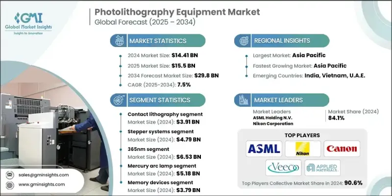
全球對智慧型手機、資料中心、人工智慧處理器和汽車電子產品中使用的更小、更快、更節能的晶片的需求激增,推動了對尖端光刻設備的投資,特別是針對 7nm 以下節點的投資。
| 市場範圍 | |
|---|---|
| 起始年份 | 2024 |
| 預測年份 | 2025-2034 |
| 起始值 | 144.1億美元 |
| 預測值 | 298億美元 |
| 複合年成長率 | 7.5% |
接觸式光刻技術需求不斷成長
2024年,接觸式微影技術佔據了相當大的佔有率,這主要得益於半導體和微加工應用,尤其是在高產量和低成本優先於極高解析度的應用領域。雖然接觸式微影技術不如更先進的光刻方法精確,但它廣泛應用於MEMS生產、印刷電路板(PCB)和某些化合物半導體製程。
步進系統的應用日益廣泛
步進式系統在2024年佔據了相當大的市場。這些系統每次曝光一個晶片,提供精確的對準和套刻控制,這對於模擬、射頻和功率裝置中使用的成熟製程技術至關重要。儘管EUV技術正在興起,但步進式系統由於其價格實惠、可靠性高,在傳統和特殊晶圓廠中仍然需求旺盛。
儲存設備將獲得發展動力
2024年,儲存設備市場將佔據相當大的佔有率,這得益於對更高密度和更快性能的需求,從而推動了對能夠處理日益複雜圖案的先進光刻設備的需求。 DRAM 和 NAND 快閃記憶體製造商依靠 DUV 和 EUV 系統來突破微縮極限,並實現 3D NAND 和 DDR5 等創新。
亞太地區將成為利潤豐厚的地區
2025年至2034年期間,亞太地區光刻設備市場將以可觀的複合年成長率成長,這得益於台灣、韓國、中國大陸和日本等半導體製造強國的崛起。這些國家擁有全球最大的晶圓代工廠和記憶體生產商,使該地區成為先進和傳統節點製造的關鍵樞紐。
光刻設備市場的主要參與者有 Gigaphoton Inc.、佳能公司、濱松光子株式會社、Veeco Instruments Inc.、EV Group (EVG)、SCREEN Semiconductor Solutions Co., Ltd.、日立高科技公司、ASML Holding NV、Xenics NVec、應用材料公司、KLA Corporation、日立高科技公司、ASML Holding NV、Xenics NVS、應用程式材料公司、KLA Corporation、Cymer LLC、S VMLA Corporation、VMLA Corporation、BMLA Corporation、Cyberim 所有Inc.。
為了鞏固其在光刻設備市場的地位,各公司正在實施以創新、可擴展性和區域擴張為重點的策略。領先的公司正在大力投資下一代技術,例如高數值孔徑 EUV 和先進的光學系統,以保持其技術優勢。同時,他們正在豐富其產品線,以滿足尖端和傳統晶圓廠的需求,確保在整個晶片生產過程中保持相關性。
目錄
第1章:方法論與範圍
第 2 章:執行摘要
第3章:行業洞察
- 產業生態系統分析
- 供應商格局
- 利潤率
- 成本結構
- 每個階段的增值
- 影響價值鏈的因素
- 中斷
- 產業衝擊力
- 成長動力
- 先進節點半導體需求激增
- 全球半導體代工產能快速擴張
- 人工智慧、物聯網和汽車電子產品的採用加速
- 向高NA EUV光刻技術過渡
- 政府主導的半導體計劃和補貼
- 產業陷阱與挑戰
- EUV系統成本極高,且複雜度極高
- 全球出口限制和地緣政治緊張局勢
- 市場機會
- 新興地區半導體工廠的擴張
- 人工智慧和機器學習在光刻製程控制中的整合
- 高數值孔徑EUV技術的發展
- 對先進封裝和 3D IC 的需求不斷成長
- 成長動力
- 成長潛力分析
- 監管格局
- 北美洲
- 歐洲
- 亞太地區
- 拉丁美洲
- 中東和非洲
- 波特的分析
- PESTEL分析
- 技術和創新格局
- 當前的技術趨勢
- 新興技術
- 價格趨勢
- 按地區
- 按產品
- 定價策略
- 新興商業模式
- 合規性要求
- 永續性措施
- 消費者情緒分析
- 專利和智慧財產權分析
- 地緣政治與貿易動態
第4章:競爭格局
- 公司介紹市佔率分析
- 公司市佔率分析
- 按地區
- 北美洲
- 歐洲
- 亞太地區
- 市場集中度分析
- 關鍵參與者的競爭基準
- 財務績效比較
- 收入
- 利潤率
- 研發
- 產品組合比較
- 產品範圍廣度
- 科技
- 創新
- 地理位置比較
- 全球足跡分析
- 服務網路覆蓋
- 各地區市場滲透率
- 競爭定位矩陣
- 領導者
- 挑戰者
- 追蹤者
- 利基市場參與者
- 戰略展望矩陣
- 財務績效比較
- 2021-2024 年關鍵發展
- 併購
- 夥伴關係與合作
- 技術進步
- 擴張和投資策略
- 永續發展舉措
- 數位轉型舉措
- 新興/新創企業競爭對手格局
第5章:市場估計與預測:依技術類型,2021 - 2034
- 接觸光刻
- 接近式光刻
- 投影光刻
- 奈米壓印光刻
- 電子束(E-beam)光刻
- 極紫外線(EUV)光刻
- 其他
第6章:市場估計與預測:按設備類型,2021 - 2034 年
- 步進系統
- 掃描器系統
- 軌道系統
- 計量和檢測工具
- 掩模對準器
- 其他
第7章:市場估計與預測:按光源,2021 - 2034 年
- 汞弧燈
- 準分子雷射
- 氟化氪(KrF)
- 氟化氬(ArF)
- 雷射產生的等離子體(LPP - 用於 EUV)
第 8 章:市場估計與預測:按應用,2021 - 2034 年
- 儲存裝置
- 邏輯積體電路
- 鑄造廠(合約製造)
- IDM(整合設備製造商)
- 類比和混合訊號積體電路
- MEMS和感測器製造
- 先進封裝(2.5D/3D IC)
- 顯示面板(LCD、OLED)
第9章:市場估計與預測:按地區,2021 - 2034
- 主要趨勢
- 北美洲
- 美國
- 加拿大
- 歐洲
- 德國
- 英國
- 法國
- 義大利
- 西班牙
- 荷蘭
- 魚子
- 亞太地區
- 中國
- 印度
- 日本
- 韓國
- 澳洲
- 亞太區
- 拉丁美洲
- 巴西
- 墨西哥
- 阿根廷
- 羅拉塔姆
- 中東和非洲
- 阿拉伯聯合大公國
- 沙烏地阿拉伯
- 南非
- 羅馬
第10章:公司簡介
- Applied Materials, Inc.
- ASML Holding NV
- Canon Inc.
- Cymer LLC (ASML subsidiary)
- DAIHEN Corporation
- EV Group (EVG)
- Gigaphoton Inc.
- Hamamatsu Photonics KK
- Hitachi High-Tech Corporation
- HOYA Corporation
- JEOL Ltd.
- KLA Corporation
- Lam Research Corporation
- Nikon Corporation
- Nova Ltd.
- Onto Innovation Inc.
- Photronics, Inc.
- SCREEN Semiconductor Solutions Co., Ltd.
- SUSS MicroTec SE
- Tokyo Electron Limited (TEL)
- Toppan Photomasks, Inc.
- Toray Industries, Inc.
- Ushio Inc.
- Veeco Instruments Inc.
- Xenics NV
The Global Photolithography Equipment Market was valued at USD 14.41 billion in 2024 and is estimated to grow at a CAGR of 7.5% to reach USD 29.8 billion by 2034.
The global surge in demand for smaller, faster, and more energy-efficient chips used in smartphones, data centers, AI processors, and automotive electronics is fueling investment in cutting-edge photolithography equipment, particularly for nodes below 7nm.
| Market Scope | |
|---|---|
| Start Year | 2024 |
| Forecast Year | 2025-2034 |
| Start Value | $14.41 Billion |
| Forecast Value | $29.8 Billion |
| CAGR | 7.5% |
Rising Demand for Contact Lithography
The contact lithography segment held a significant share in 2024, driven by semiconductor and microfabrication applications, particularly where high throughput and lower costs are prioritized over extreme resolution. While it lacks the precision of more advanced lithography methods, contact lithography is widely used in MEMS production, printed circuit boards (PCBs), and certain compound semiconductor processes.
Increasing Adoption of Stepper Systems
The stepper systems segment generated a substantial share in 2024. These systems expose one die at a time, providing precise alignment and overlay control, which is critical for mature process technologies used in analog, RF, and power devices. Despite the rise of EUV, steppers remain in strong demand due to their affordability and reliability across legacy and specialty fabs.
Memory Devices to Gain Traction
The memory devices segment held a sizeable share in 2024, driven by the need for higher density and faster performance, which is driving demand for advanced photolithography equipment capable of handling increasingly complex patterns. DRAM and NAND flash manufacturers rely on both DUV and EUV systems to push scaling limits and enable innovations such as 3D NAND and DDR5.
Asia Pacific to Emerge as a Lucrative Region
Asia Pacific photolithography equipment market will grow at a decent CAGR during 2025-2034, driven by the presence of semiconductor manufacturing powerhouses such as Taiwan, South Korea, China, and Japan. These countries host the world's largest foundries and memory producers, making the region a critical hub for both advanced and legacy node manufacturing.
Major players in the photolithography equipment market are Gigaphoton Inc., Canon Inc., Hamamatsu Photonics K.K., Veeco Instruments Inc., EV Group (EVG), SCREEN Semiconductor Solutions Co., Ltd., Hitachi High-Tech Corporation, ASML Holding N.V., Xenics NV, Applied Materials, Inc., KLA Corporation, Cymer LLC, SUSS MicroTec SE, Nikon Corporation, Ushio Inc., Lam Research Corporation, and Onto Innovation Inc.
To solidify their position in the photolithography equipment market, companies are executing strategies focused on innovation, scalability, and regional expansion. Leading firms are investing heavily in next-generation technologies such as high-NA EUV and advanced optical systems to maintain their technological edge. At the same time, they are diversifying their offerings to cater to both leading-edge and legacy fabs, ensuring relevance across the full spectrum of chip production.
Table of Contents
Chapter 1 Methodology and Scope
- 1.1 Market scope and definition
- 1.2 Research design
- 1.2.1 Research approach
- 1.2.2 Data collection methods
- 1.3 Data mining sources
- 1.3.1 Global
- 1.3.2 Regional/Country
- 1.4 Base estimates and calculations
- 1.4.1 Base year calculation
- 1.4.2 Key trends for market estimation
- 1.5 Primary research and validation
- 1.5.1 Primary sources
- 1.6 Forecast model
- 1.7 Research assumptions and limitations
Chapter 2 Executive Summary
- 2.1 Industry 3600 synopsis
- 2.2 Key market trends
- 2.2.1. Technology type
- 2.2.2 Equipment type
- 2.2.3 Wavelength
- 2.2.4 Light source
- 2.2.5 Application
- 2.2.6 North America
- 2.2.7 Europe
- 2.2.8 Asia Pacific
- 2.2.9 Latin America
- 2.2.10 Middle East & Africa
- 2.3 TAM Analysis, 2025-2034 (USD Million)
- 2.4 CXO perspectives: Strategic imperatives
- 2.5 Executive decision points
- 2.6 Critical success factors
- 2.7 Future outlook and strategic recommendations
Chapter 3 Industry Insights
- 3.1 Industry ecosystem analysis
- 3.1.1 Supplier landscape
- 3.1.2 Profit margin
- 3.1.3 Cost structure
- 3.1.4 Value addition at each stage
- 3.1.5 Factor affecting the value chain
- 3.1.6 Disruptions
- 3.2 Industry impact forces
- 3.2.1 Growth drivers
- 3.2.1.1 Surging demand for advanced-node semiconductors
- 3.2.1.2 Rapid expansion of global semiconductor foundry capacity
- 3.2.1.3 Acceleration in AI, IoT, and automotive electronics adoption
- 3.2.1.4 Transition toward High-NA EUV lithography
- 3.2.1.5 Government-led semiconductor initiatives and subsidies
- 3.2.2 Industry pitfalls and challenges
- 3.2.2.1 Extremely high cost and complexity of EUV systems
- 3.2.2.2 Global export restrictions and geopolitical tensions
- 3.2.3 Market opportunities
- 3.2.3.1 Expansion of semiconductor fabs in emerging regions
- 3.2.3.2 Integration of AI and machine learning in lithography process control
- 3.2.3.3 Development of High-NA EUV technology
- 3.2.3.4 Growing demand for advanced packaging and 3D ICs
- 3.2.1 Growth drivers
- 3.3 Growth potential analysis
- 3.4 Regulatory landscape
- 3.4.1 North America
- 3.4.2 Europe
- 3.4.3 Asia Pacific
- 3.4.4 Latin America
- 3.4.5 Middle East & Africa
- 3.5 Porter’s analysis
- 3.6 PESTEL analysis
- 3.7 Technological and innovation landscape
- 3.7.1 Current technological trends
- 3.7.2 Emerging technologies
- 3.8 Price trends
- 3.8.1 By region
- 3.8.2 By product
- 3.9 Pricing strategies
- 3.10 Emerging business models
- 3.11 Compliance requirements
- 3.12 Sustainability measures
- 3.13 Consumer sentiment analysis
- 3.14 Patent and IP analysis
- 3.15 Geopolitical and trade dynamics
Chapter 4 Competitive Landscape, 2024
- 4.1 Introduction company market share analysis
- 4.2 Company market share analysis
- 4.2.1 By region
- 4.2.1. North America
- 4.2.2. Europe
- 4.2.3. Asia Pacific
- 4.2.2 Market concentration analysis
- 4.3 Competitive benchmarking of key players
- 4.3.1 Financial performance comparison
- 4.3.1.1. Revenue
- 4.3.1.2. Profit margin
- 4.3.1.3. R&D
- 4.3.2 Product portfolio comparison
- 4.3.2.1. Product range breadth
- 4.3.2.2. Technology
- 4.3.2.3. Innovation
- 4.3.3 Geographic presence comparison
- 4.3.3.1. Global footprint analysis
- 4.3.3.2. Service network coverage
- 4.3.3.3. Market penetration by region
- 4.3.4 Competitive positioning matrix
- 4.3.4.1. Leaders
- 4.3.4.2. Challengers
- 4.3.4.3. Followers
- 4.3.4.4. Niche players
- 4.3.5 Strategic outlook matrix
- 4.3.1 Financial performance comparison
- 4.4 Key developments, 2021-2024
- 4.4.1 Mergers and acquisitions
- 4.4.2 Partnerships and collaborations
- 4.4.3 Technological advancements
- 4.4.4 Expansion and investment strategies
- 4.4.5 Sustainability initiatives
- 4.4.6 Digital transformation initiatives
- 4.5 Emerging/ startup competitors landscape
Chapter 5 Market Estimates & Forecast, By Technology Type, 2021 - 2034 (USD Million)
- 5.1 Contact lithography
- 5.2 Proximity lithography
- 5.3 Projection lithography
- 5.4 Nanoimprint lithography
- 5.5 Electron beam (E-beam) lithography
- 5.6 Extreme ultraviolet (EUV) lithography
- 5.7 Others
Chapter 6 Market estimates & forecast, By Equipment Type, 2021 - 2034 (USD Million)
- 6.1 Stepper systems
- 6.2 Scanner systems
- 6.3 Track systems
- 6.4 Metrology & inspection tools
- 6.5 Mask aligners
- 6.6 Others
Chapter 7 Market estimates & forecast, By Light Source, 2021 - 2034 (USD Million)
- 7.1 Mercury arc lamp
- 7.2 Excimer laser
- 7.3 Krypton fluoride (KrF)
- 7.4 Argon fluoride (ArF)
- 7.5 Laser-produced plasma (LPP - for EUV)
Chapter 8 Market Estimates and Forecast, By Application, 2021 - 2034 ( USD Million)
- 8.1 Memory devices
- 8.2 Logic ICs
- 8.3 Foundry (Contract manufacturing)
- 8.4 IDMs (Integrated Device Manufacturers)
- 8.5 Analog & mixed signal ICs
- 8.6 MEMS & sensor fabrication
- 8.7 Advanced packaging (2.5D / 3D ICs)
- 8.8 Display panels (LCD, OLED)
Chapter 9 Market Estimates and Forecast, By Region, 2021 - 2034 (USD Million)
- 9.1 Key trends
- 9.2 North America
- 9.2.1 U.S.
- 9.2.2 Canada
- 9.3 Europe
- 9.3.1 Germany
- 9.3.2 U.K.
- 9.3.3 France
- 9.3.4 Italy
- 9.3.5 Spain
- 9.3.6 Netherlands
- 9.3.7 ROE
- 9.4 Asia Pacific
- 9.4.1 China
- 9.4.2 India
- 9.4.3 Japan
- 9.4.4 South Korea
- 9.4.5 Australia
- 9.4.6 RoAPAC
- 9.5 Latin America
- 9.5.1 Brazil
- 9.5.2 Mexico
- 9.5.3 Argentina
- 9.5.4 RoLATAM
- 9.6 Middle East & Africa
- 9.6.1 UAE
- 9.6.2 Saudi Arabia
- 9.6.3 South Africa
- 9.6.4 RoMEA
Chapter 10 Company Profile
- 10.1 Applied Materials, Inc.
- 10.2 ASML Holding N.V.
- 10.3 Canon Inc.
- 10.4 Cymer LLC (ASML subsidiary)
- 10.5 DAIHEN Corporation
- 10.6 EV Group (EVG)
- 10.7 Gigaphoton Inc.
- 10.8 Hamamatsu Photonics K.K.
- 10.9 Hitachi High-Tech Corporation
- 10.10 HOYA Corporation
- 10.11 JEOL Ltd.
- 10.12 KLA Corporation
- 10.13 Lam Research Corporation
- 10.14 Nikon Corporation
- 10.15 Nova Ltd.
- 10.16 Onto Innovation Inc.
- 10.17 Photronics, Inc.
- 10.18 SCREEN Semiconductor Solutions Co., Ltd.
- 10.19 SUSS MicroTec SE
- 10.20 Tokyo Electron Limited (TEL)
- 10.21 Toppan Photomasks, Inc.
- 10.22 Toray Industries, Inc.
- 10.23 Ushio Inc.
- 10.24 Veeco Instruments Inc.
- 10.25 Xenics NV
 微影術設備市場-2026-2032年全球市場預測
 微影術設備市場規模、佔有率和成長分析:按技術、設備類型、光源、應用、節點尺寸、最終用戶和地區分類-2026-2033年產業預測
 微影術設備市場規模、佔有率、趨勢和預測:按製程、波長、裝置波長、應用、最終用途和地區分類,2026-2034年
 全球微影術設備市場規模、佔有率、趨勢和成長分析報告(2026-2034年)
 微影術設備市場規模、佔有率和趨勢分析報告:按製程、光源、波長、應用、地區和細分市場分類(2026-2033 年)
 2026年全球微影術設備市場報告2026年全球半導體對準器市場報告
 微影術設備市場-全球產業規模、佔有率、趨勢、機會和預測:按類型、深紫外線類型、波長、裝置波長、最終用途、應用、地區和競爭格局分類,2021-2031年193nm準分子雷射市場:按雷射類型、功率輸出、銷售管道和應用分類 - 全球預測(2026-2032)半導體微影術設備市場:未來預測(2025-2030)