


 |
市場調查報告書
商品編碼
1773475
硫族化物(MoS2、WS2、WSe2)市場機會、成長動力、產業趨勢分析及 2025 - 2034 年預測Chalcogenides (MoS2, WS2, WSe2) Market Opportunity, Growth Drivers, Industry Trend Analysis, and Forecast 2025 - 2034 |
||||||
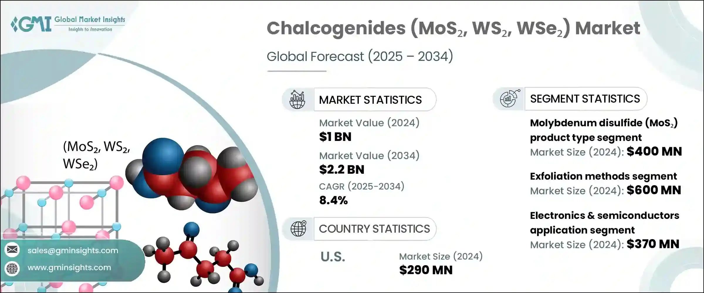
2024 年全球硫族化物(MoS2、WS2、WSe2)市場價值為 10 億美元,預計到 2034 年將以 8.4% 的複合年成長率成長至 22 億美元。這種穩定成長反映了先進材料領域的廣泛發展勢頭,這一領域受到奈米技術的發展以及多個垂直領域對高性能、節能解決方案日益成長的需求的推動。這些層狀過渡金屬二硫族化物由於其卓越的電氣、機械和光學性能,已成為未來電子產品的關鍵推動因素。由於傳統的矽基技術遇到物理和縮放限制,這些2D材料正成為微型電子產品、軟性設備和高速電晶體等應用領域的有希望的替代品。人們對緊湊且節能的硬體日益成長的興趣在航太、國防、電信和醫療設備等領域尤為重要。
包括美國、亞太地區和歐盟在內的各地區政府支持的研發計畫正在提供關鍵的資金和機構支持,以推動下一代材料創新。這些計劃包括建立國家創新中心、資助試點製造中心以及支持實驗室規模研究的商業化。公私合作夥伴關係正在加強,尤其是在半導體和再生能源領域,將2D半導體整合到軟性基板中正變得越來越可行。該行業正在響應對更快、更小、更節能的晶片日益成長的需求,而二硫化鉬和二氧化鎢等材料由於其可調能隙和卓越的載流子遷移率,相比傳統材料具有顯著的性能優勢。
| 市場範圍 | |
|---|---|
| 起始年份 | 2024 |
| 預測年份 | 2025-2034 |
| 起始值 | 10億美元 |
| 預測值 | 22億美元 |
| 複合年成長率 | 8.4% |
在製造技術中,剝離法細分市場在2024年創造了6億美元的市場規模,預計到2034年將以7.9%的複合年成長率成長。雖然剝離法對於研究級材料和原型仍然至關重要,但化學氣相沉積 (CVD) 技術因其能夠產生與商用級半導體製程相容的均勻高品質薄膜,正日益成為可擴展生產領域的主導。 CVD 技術能夠實現精確的層控制、廣泛的基材相容性以及工業規模的可重複性,使其成為從研發過渡到高通量電子製造的首選技術。許多製造實驗室和中試設施已採用 CVD 技術,凸顯了其在連接實驗室創新與奈米材料商業規模應用方面的關鍵作用。
電子和半導體領域在2024年創造了可觀的收入。其獨特的能帶結構和半導體特性使其成為先進場效電晶體、儲存元件和薄膜邏輯電路的理想候選材料。這些材料具有前所未有的靈活性和超薄架構,使其成為下一代穿戴式技術、整合光子學和軟體機器人的理想選擇。研究人員已經報告了其開關行為和閾值性能,其性能堪比甚至超越了規模化矽基裝置,這促使各大半導體製造商在邁向後莫耳定律設計時代之際,紛紛探索這些2D替代方案。
預計在2025年至2034年期間,美國硫族化合物(二硫化鉬、二硫化鎢和二硒化鎢)市場將以顯著的複合年成長率成長,這主要得益於研發投入,尤其是在量子技術和國防級半導體領域的應用。儘管二硫化鉬和二硒化鎢等塊狀材料主要從亞洲進口,但美國在下游開發和整合方面處於領先地位,並向國際市場出口增值衍生物。美國的高科技產業將這些材料應用於尖端原型設計,不斷突破光電子學、光子學和下一代電晶體架構的界限。 ACS Material和2D Tech等公司在推動國內研究工作方面發揮關鍵作用,而大型國防承包商和電子產品製造商則推動對這些高性能奈米材料的需求。
全球硫族化物(MoS2、WS2、WSe2)市場知名的企業包括SixCarbon Technology、Graphene Laboratories Inc.、American Elements、ACS Material LLC和XFNANO Materials Tech Co., Ltd.。這些公司對於材料合成和供應鏈開發都至關重要。為了提升市場地位並擴大全球影響力,硫族化物產業的領導企業正在採取多種策略。他們正在擴大生產能力以滿足日益成長的工業和商業需求,同時繼續投資於高精度材料表徵和客製化。與學術機構和國家實驗室的合作有助於促進尖端創新,尤其是在量子應用和軟性電子領域。主要企業也正在與設備製造商建立策略合作夥伴關係,共同開發使用2D材料的特定應用解決方案。
目錄
第1章:方法論
- 市場範圍和定義
- 研究設計
- 研究方法
- 資料收集方法
- 資料探勘來源
- 全球的
- 地區/國家
- 基礎估算與計算
- 基準年計算
- 市場評估的主要趨勢
- 初步研究和驗證
- 主要來源
- 預測模型
- 研究假設和局限性
第2章:執行摘要
第3章:行業洞察
- 產業生態系統分析
- 供應商概況
- 利潤率
- 每個階段的增值
- 影響價值鏈的因素
- 中斷
- 產業衝擊力
- 成長動力
- 產業陷阱與挑戰
- 市場機會
- 成長潛力分析
- 監管格局
- 北美洲
- 歐洲
- 亞太地區
- 拉丁美洲
- 中東和非洲
- 波特的分析
- PESTEL分析
- 價格趨勢
- 按地區
- 按產品
- 未來市場趨勢
- 技術和創新格局
- 當前的技術趨勢
- 新興技術
- 專利態勢
- 貿易統計資料(HS 編碼)(註:僅提供主要國家的貿易統計數據
- 主要進口國
- 主要出口國
- 永續性和環境方面
- 永續實踐
- 減少廢棄物的策略
- 生產中的能源效率
- 環保舉措
- 碳足跡考量
第4章:競爭格局
- 介紹
- 公司市佔率分析
- 按地區
- 北美洲
- 歐洲
- 亞太地區
- 拉丁美洲
- MEA
- 按地區
- 公司矩陣分析
- 主要市場參與者的競爭分析
- 競爭定位矩陣
- 關鍵進展
- 併購
- 夥伴關係與合作
- 新產品發布
- 擴張計劃
第5章:市場估計與預測:依材料類型,2021-2034
- 主要趨勢
- 二硫化鉬(MoS2)
- 二硫化鎢(WS2)
- 二硒化鎢(WSe2)
- 異質結構和混合結構
- 其他
第6章:市場估計與預測:依合成與製造技術,2021-2034 年
- 主要趨勢
- 去角質方法
- 機械剝落
- 液相剝離
- 電化學剝離
- 插層輔助剝離
- 其他
- 化學氣相沉積(CVD)
- 傳統 CVD 工藝
- 金屬有機化學氣相沉積 (MOCVD)
- 物理氣相沉積(PVD)
- 濺鍍技術
- 脈衝雷射沉積
- 可擴展的生產方法
- 化學合成路線
- 其他
第7章:市場估計與預測:按應用,2021-2034
- 主要趨勢
- 電子和半導體
- 場效電晶體(FET)
- 邏輯閘和電路
- 儲存裝置
- 軟性電子產品
- 其他
- 光電子學與光子學
- 光電探測器
- 發光二極體 (LED)
- 電致發光裝置
- 太陽能電池/光伏
- 其他
- 能量儲存與轉換
- 可充電電池
- 超級電容器
- 析氫反應(HER)催化劑
- 二氧化碳還原催化劑
- 熱電裝置
- 燃料電池
- 其他
- 感測器和探測器
- 氣體感測器
- 生物感測器
- 壓力和應變感測器
- 其他
- 量子技術
- 摩擦學和潤滑劑
- 生物醫學應用
- 其他
第8章:市場估計與預測:按地區,2021-2034
- 主要趨勢
- 北美洲
- 美國
- 加拿大
- 歐洲
- 德國
- 英國
- 法國
- 義大利
- 西班牙
- 歐洲其他地區
- 亞太地區
- 中國
- 印度
- 日本
- 澳洲
- 韓國
- 亞太其他地區
- 拉丁美洲
- 巴西
- 墨西哥
- 阿根廷
- 拉丁美洲其他地區
- 中東和非洲
- 沙烏地阿拉伯
- 南非
- 阿拉伯聯合大公國
- 中東和非洲其他地區
第9章:公司簡介
- 2D Semiconductors
- 6Carbon Technology
- ACS Material, LLC
- Applied Nanolayers BV
- Grolltex Inc.
- HQ Graphene
- Muke Nano
- Nanoshel LLC
- SixCarbon Technology
- Ossila Ltd.
- SVT Associates, Inc.
- Tungsten Compounds GmbH
- XFNANO Materials Tech Co., Ltd.
- Intelligent Materials Pvt. Ltd.
- American Elements
- Graphene Laboratories Inc.
- MSE Supplies LLC
- Sigma-Aldrich (Merck KGaA)
- Stanford Advanced Materials
- Edgetech Industries LLC
The Global Chalcogenides (MoS2, WS2, WSe2) Market was valued at USD 1 billion in 2024 and is estimated to grow at a CAGR of 8.4% to reach USD 2.2 billion by 2034. This steady growth reflects broader momentum in the advanced materials sector, which is being propelled by developments in nanotechnology and the increasing demand for high-performance, energy-efficient solutions across several verticals. These layered transition metal dichalcogenides have become key enablers in future electronics due to their exceptional electrical, mechanical, and optical behavior. As traditional silicon-based technologies encounter physical and scaling limitations, these 2D materials are emerging as promising alternatives in applications such as miniaturized electronics, flexible devices, and high-speed transistors. The growing interest in compact and power-efficient hardware is particularly relevant in sectors like aerospace, defense, telecommunications, and medical devices.
Government-backed R&D initiatives across regions, including the US, Asia-Pacific, and the EU, are providing crucial financial and institutional support to push next-generation material innovation. This includes establishing national innovation centers, funding pilot manufacturing hubs, and supporting the commercialization of lab-scale research. Public-private partnerships are intensifying, particularly in the semiconductor and renewable energy domains, where the integration of 2D semiconductors into flexible substrates is becoming more feasible. The industry is responding to the growing demand for faster, smaller, and energy-optimized chips, where materials such as MoS2 and WS2 offer considerable performance advantages over legacy materials due to their tunable bandgap and superior carrier mobility.
| Market Scope | |
|---|---|
| Start Year | 2024 |
| Forecast Year | 2025-2034 |
| Start Value | $1 billion |
| Forecast Value | $2.2 billion |
| CAGR | 8.4% |
Among fabrication techniques, the exfoliation methods segment generated USD 0.6 billion in 2024 and is predicted to grow at a CAGR of 7.9% through 2034. While exfoliation remains critical for research-grade materials and prototypes, chemical vapor deposition (CVD) is increasingly dominating scalable production due to its ability to yield uniform and high-quality thin films compatible with commercial-grade semiconductor processes. CVD enables precise layer control, broad substrate compatibility, and reproducibility at industrial volumes, which positions it as the technology of choice for transitioning from R&D to high-throughput electronics manufacturing. Many fabrication labs and pilot facilities have adopted CVD, underlining its pivotal role in bridging lab innovations with commercial-scale applications in nanomaterials.
The electronics & semiconductor segment generated notable revenues in 2024. Their unique band structure and semiconducting properties make them excellent candidates for advanced field-effect transistors, memory devices, and thin-film logic circuits. These materials allow for unprecedented flexibility and ultra-thin architectures, making them highly desirable for next-gen wearable technology, integrated photonics, and soft robotics. Researchers have already reported switching behaviors and threshold performances that match or exceed those of scaled silicon-based devices, which is pushing major semiconductor manufacturers to explore these 2D alternatives as they approach post-Moore's Law design eras.
United States Chalcogenides (MoS2, WS2, and WSe2) Market is estimated to grow at a notable CAGR during 2025-2034, driven by R&D, especially for applications in quantum technology and defense-grade semiconductors. Although bulk materials like MoS2 and WSe2 are largely imported from Asia, the U.S. leads in downstream development and integration, exporting value-added derivatives to international markets. High-tech industries in the U.S. utilize these materials in cutting-edge prototyping, pushing boundaries in optoelectronics, photonics, and next-generation transistor architecture. Companies such as ACS Material and 2D Tech play a critical role in enabling domestic research efforts, while large defense contractors and electronics manufacturers drive demand for these high-performance nanomaterials.
Prominent industry players operating in the Global Chalcogenides (MoS2, WS2, WSe2) market include SixCarbon Technology, Graphene Laboratories Inc., American Elements, ACS Material LLC, and XFNANO Materials Tech Co., Ltd. These companies are integral to both material synthesis and supply chain development. To enhance their market position and expand global reach, leading firms in the chalcogenides industry are leveraging several strategies. They are scaling up production capabilities to meet growing industrial and commercial demand while continuing to invest in high-precision material characterization and customization. Collaborations with academic institutions and national laboratories help foster cutting-edge innovation, particularly in quantum applications and flexible electronics. Key players are also entering strategic partnerships with device manufacturers to co-develop application-specific solutions using 2D materials.
Table of Contents
Chapter 1 Methodology
- 1.1 Market scope and definition
- 1.2 Research design
- 1.2.1 Research approach
- 1.2.2 Data collection methods
- 1.3 Data mining sources
- 1.3.1 Global
- 1.3.2 Regional/Country
- 1.4 Base estimates and calculations
- 1.4.1 Base year calculation
- 1.4.2 Key trends for market estimation
- 1.5 Primary research and validation
- 1.5.1 Primary sources
- 1.6 Forecast model
- 1.7 Research assumptions and limitations
Chapter 2 Executive Summary
- 2.1 Industry 3600 synopsis
- 2.2 Key market trends
- 2.2.1 Regional
- 2.2.2 Material Type
- 2.2.3 Application
- 2.3 TAM Analysis, 2025-2034
- 2.4 CXO perspectives: Strategic imperatives
- 2.4.1 Executive decision points
- 2.4.2 Critical success factors
- 2.5 Future Outlook and Strategic Recommendations
Chapter 3 Industry Insights
- 3.1 Industry ecosystem analysis
- 3.1.1 Supplier Landscape
- 3.1.2 Profit Margin
- 3.1.3 Value addition at each stage
- 3.1.4 Factor affecting the value chain
- 3.1.5 Disruptions
- 3.2 Industry impact forces
- 3.2.1 Growth drivers
- 3.2.2 Industry pitfalls and challenges
- 3.2.3 Market opportunities
- 3.3 Growth potential analysis
- 3.4 Regulatory landscape
- 3.4.1 North America
- 3.4.2 Europe
- 3.4.3 Asia Pacific
- 3.4.4 Latin America
- 3.4.5 Middle East & Africa
- 3.5 Porter's analysis
- 3.6 PESTEL analysis
- 3.6.1 Technology and Innovation landscape
- 3.6.2 Current technological trends
- 3.6.3 Emerging technologies
- 3.7 Price trends
- 3.7.1 By region
- 3.7.2 By product
- 3.8 Future market trends
- 3.9 Technology and Innovation landscape
- 3.9.1 Current technological trends
- 3.9.2 Emerging technologies
- 3.10 Patent Landscape
- 3.11 Trade statistics (HS code)
- 3.11.1 Major importing countries
- 3.11.2 Major exporting countries
- 3.12 Sustainability and Environmental Aspects
- 3.12.1 Sustainable Practices
- 3.12.2 Waste Reduction Strategies
- 3.12.3 Energy Efficiency in Production
- 3.12.4 Eco-friendly Initiatives
- 3.13 Carbon Footprint Considerations
Chapter 4 Competitive Landscape, 2024
- 4.1 Introduction
- 4.2 Company market share analysis
- 4.2.1 By region
- 4.2.1.1 North America
- 4.2.1.2 Europe
- 4.2.1.3 Asia Pacific
- 4.2.1.4 LATAM
- 4.2.1.5 MEA
- 4.2.1 By region
- 4.3 Company matrix analysis
- 4.4 Competitive analysis of major market players
- 4.5 Competitive positioning matrix
- 4.6 Key developments
- 4.6.1 Mergers & acquisitions
- 4.6.2 Partnerships & collaborations
- 4.6.3 New Product Launches
- 4.6.4 Expansion Plans
Chapter 5 Market Estimates & Forecast, By Material Type, 2021-2034 (USD Million) (Kilo Tons)
- 5.1 Key trends
- 5.2 Molybdenum Disulfide (MoS2)
- 5.3 Tungsten Disulfide (WS2)
- 5.4 Tungsten Diselenide (WSe2)
- 5.5 Heterostructures & Hybrids
- 5.6 Others
Chapter 6 Market Estimates & Forecast, By Synthesis & Manufacturing Technologies, 2021-2034 (USD Million) (Kilo Tons)
- 6.1 Key trends
- 6.2 Exfoliation methods
- 6.2.1 Mechanical exfoliation
- 6.2.2 Liquid-phase exfoliation
- 6.2.3 Electrochemical exfoliation
- 6.2.4 Intercalation-assisted exfoliation
- 6.2.5 Others
- 6.3 Chemical vapor deposition (CVD)
- 6.3.1 Conventional CVD processes
- 6.3.2 Metal-organic CVD (MOCVD)
- 6.4 Physical vapor deposition (PVD)
- 6.4.1 Sputtering techniques
- 6.4.2 Pulsed laser deposition
- 6.4.3 Scalable production methods
- 6.5 Chemical synthesis routes
- 6.6 Others
Chapter 7 Market Estimates & Forecast, By Application, 2021-2034 (USD Million) (Kilo Tons)
- 7.1 Key trends
- 7.2 Electronics & semiconductors
- 7.2.1 Field-effect transistors (FETs)
- 7.2.2 Logic gates & circuits
- 7.2.3 Memory devices
- 7.2.4 Flexible electronics
- 7.2.5 Others
- 7.3 Optoelectronics & photonics
- 7.3.1 Photodetectors
- 7.3.2 Light-emitting diodes (LEDs)
- 7.3.3 Electroluminescent devices
- 7.3.4 Solar cells / photovoltaics
- 7.3.5 Others
- 7.4 Energy storage & conversion
- 7.4.1 Rechargeable batteries
- 7.4.2 Supercapacitors
- 7.4.3 Hydrogen evolution reaction (HER) catalysts
- 7.4.4 Co2 reduction catalysts
- 7.4.5 Thermoelectric devices
- 7.4.6 Fuel cells
- 7.4.7 Others
- 7.5 Sensors & detectors
- 7.5.1 Gas sensors
- 7.5.2 Biosensors
- 7.5.3 Pressure & strain sensors
- 7.5.4 Others
- 7.6 Quantum technologies
- 7.7 Tribology & lubricants
- 7.8 Biomedical applications
- 7.9 Others
Chapter 8 Market Estimates & Forecast, By Region, 2021-2034 (USD Million) (Kilo Tons)
- 8.1 Key trends
- 8.2 North America
- 8.2.1 U.S.
- 8.2.2 Canada
- 8.3 Europe
- 8.3.1 Germany
- 8.3.2 UK
- 8.3.3 France
- 8.3.4 Italy
- 8.3.5 Spain
- 8.3.6 Rest of Europe
- 8.4 Asia Pacific
- 8.4.1 China
- 8.4.2 India
- 8.4.3 Japan
- 8.4.4 Australia
- 8.4.5 South Korea
- 8.4.6 Rest of Asia Pacific
- 8.5 Latin America
- 8.5.1 Brazil
- 8.5.2 Mexico
- 8.5.3 Argentina
- 8.5.4 Rest of Latin America
- 8.6 Middle East & Africa
- 8.6.1 Saudi Arabia
- 8.6.2 South Africa
- 8.6.3 UAE
- 8.6.4 Rest of Middle East & Africa
Chapter 9 Company Profiles
- 9.1 2D Semiconductors
- 9.2 6Carbon Technology
- 9.3 ACS Material, LLC
- 9.4 Applied Nanolayers B.V.
- 9.5 Grolltex Inc.
- 9.6 HQ Graphene
- 9.7 Muke Nano
- 9.8 Nanoshel LLC
- 9.9 SixCarbon Technology
- 9.10 Ossila Ltd.
- 9.11 SVT Associates, Inc.
- 9.12 Tungsten Compounds GmbH
- 9.13 XFNANO Materials Tech Co., Ltd.
- 9.14 Intelligent Materials Pvt. Ltd.
- 9.15 American Elements
- 9.16 Graphene Laboratories Inc.
- 9.17 MSE Supplies LLC
- 9.18 Sigma-Aldrich (Merck KGaA)
- 9.19 Stanford Advanced Materials
- 9.20 Edgetech Industries LLC
 奈米材料市場按類型、合成技術、形態、應用和最終用途產業分類-全球預測,2025-2032
 奈米材料的全球市場(2025年)- 終端用戶,用途,競爭企業:2024年~2030年的分析與預測
 2025年二氧化鈦奈米材料全球市場報告2025年全球智慧奈米建築材料市場報告2025年全球智慧奈米材料市場報告2025年全球奈米材料市場報告
 二氧化鈦奈米材料市場報告(按類型、應用和地區)2025-2033
 2032 年奈米材料市場預測:按產品類型、結構類型、材料類型、應用和地區進行的全球分析
 奈米材料市場 - 預測 2025-20302025 年至 2033 年奈米化學品市場規模、佔有率、趨勢及預測(按類型、應用和地區)