


 |
市場調查報告書
商品編碼
1433831
GaAs晶圓(砷化鎵晶圓):市場佔有率分析、產業趨勢、成長預測(2024-2029)Gallium Arsenide GaAs Wafer - Market Share Analysis, Industry Trends & Statistics, Growth Forecasts (2024 - 2029) |
||||||
※ 本網頁內容可能與最新版本有所差異。詳細情況請與我們聯繫。
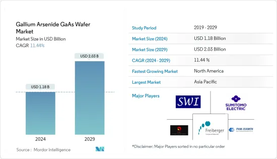
GaAs晶圓(砷化鎵晶圓)市場規模預計到2024年為11.8億美元,預計到2029年將達到20.3億美元,在預測期內(2024-2029年)複合年成長率為11.44%,預計將成長。
GaAs 常用於電子領域,主要用於半導體製造。 LED、雷射二極體、光電元件和單晶微波積體電路等產品擴大採用 GaAs 晶圓,這被認為是推動所研究市場成長的關鍵因素之一。調節這種化合物的價格將增加砷化鎵晶圓製造商的成長機會。
砷化鎵或GaAs是一種由兩種元素組成的化合物材料。用於製造砷化鎵晶圓的半導體是直接能隙半導體,在光電元件中特別有用,因為它們允許電子快速穿過組件而沒有太多干擾。
智慧型手機和運算設備的普及以及普通照明中發光二極體(LED) 的日益普及是該市場的主要成長動力。此外,物聯網的出現也是擴大市場趨勢的主要因素。這項技術也創造了對採用砷化鎵 IC 的射頻通訊設備的需求。
因此,隨著多家電信業者擴大其通訊基礎設施,對 GaAs 晶圓的需求可能會增加,從而對未來幾年的研究市場成長產生積極影響。此外,GaAs晶圓的獨特特性增加了電子、航太和國防、通訊各個最終用戶產業對GaAs晶圓的需求,也推動了全球對GaAs晶圓的需求。
例如,砷化鎵晶圓是一種寬直接能隙材料,可抵抗輻射損傷,使其成為高功率太空電子和光學窗口的理想選擇,為市場拓展以及電子戰系統、電動飛機等提供了機會。產生新的市場趨勢和使用案例,包括在寬頻行動電話網路技術的開發中增加採用。
然而,GaAs晶圓的價格是其主要缺點之一,這也解釋了其使用率低的原因。為了解決這些問題,研究人員創造了生產低成本砷化鎵薄膜的新方法,可以幫助製造替代矽的設備,支持研究市場的成長。
COVID-19大流行的全球爆發以及各國政府隨後採取的遏制病毒傳播的果斷行動對半導體行業產生了顯著影響,影響了半導體零件的製造並影響了客戶需求,從而抑制了全球市場生長。然而,數位技術的普及顯著增加了對先進消費性電子產品以及支持它們的數位基礎設施的需求,對所研究市場的成長產生了積極影響。
GaAs晶圓市場趨勢
射頻電子佔據很大的市場佔有率
在砷化鎵基板上製造的射頻元件廣泛應用於無線網路(WLAN)、4G/5G基地台、行動通訊、衛星通訊和Wi-Fi通訊無線通訊應用。這些發展代表了支援 4G 和 5G 服務的智慧型手機和其他行動裝置所需的下一代超緊湊高效能射頻前端晶片組開發的一個重要里程碑。
此外,GaAs晶圓更高的效率和低耗電量正在鼓勵參與企業採用它們,這對GaAs晶圓的需求產生積極影響。光電裝置先前廣泛應用於電腦周邊設備和短程光纖通訊。儘管如此,擴增實境(AR)、LiDAR和臉部辨識等新應用對其的需求仍然很高。
在全球範圍內,網路普及不斷提高,特別是在印度和巴西等發展中國家,刺激了對砷化鎵晶圓的需求。此後,光纖網路、回程傳輸、基地台和無線通訊基礎設施對Wi-Fi連接產品的需求不斷增加,並支援了網路在全球的普及。
此外,不斷成長的行動資料消耗率和物聯網設備的廣泛採用也推動了對 Wi-Fi 和其他無線通訊設備的需求。這些產品和無線通訊技術的高成長率正在推動砷化鎵晶圓的採用。例如,根據 5G America 的數據,全球行動 5G 用戶數量預計將從 2023 年的 190 萬增加到 2027 年的 590 萬。
亞太地區將在預測期內主導市場
亞太地區對智慧消費性電子產品的需求不斷成長。中國、台灣、日本和印度對智慧型手機、穿戴式裝置、電腦和筆記型電腦等先進科技設備的需求正在迅速成長,進一步加速了該地區的市場成長。與矽基設備相比,砷化鎵產品提供了改進的資料傳輸和質量,從而提高了連接性並增加了需求。此外,砷化鎵產品可以大規模生產,良產量比率,這也促進了業務成長。網際網路的普及、4G和5G網路的擴展以及電子工業也有望推動該地區GaAs晶圓市場的開拓。
亞太地區的關鍵促進因素之一是對計算設備、智慧型手機、平板電腦和筆記型電腦等先進技術設備的需求不斷成長。電晶體等 GaAs 產品可用於智慧型手機和其他無線通訊設備,因此不斷成長的需求正以令人鼓舞的速度推動對 GaAs 晶圓的需求。
中國是主導電子產業市場的大國,這得益於政府的大力支持,推動中國科研市場的開拓。例如,中國政府透過向產業相關人員提供資金來促進國內技術市場的發展。這些趨勢鼓勵新參與企業擴大在該國的業務。例如,2023年2月,GaAs晶圓基板等化合物半導體晶圓基板製造商AXT宣布擴建北京工廠。該公司投資了原料萃取設備,以進一步鞏固其作為化合物半導體基板領先供應商的地位。
中國也是5G基礎設施發展以及其他消費性電子和電動車解決方案採用的領先國家之一。例如,根據工信部的數據,到年終,中國將擁有約231萬個5G基地台。隨著這些產業的發展,中國研究市場的成長前景正在顯現。
台灣正見證晶圓市場是科技發展的關鍵領域之一。因此,台灣預計也將在全球砷化鎵晶圓市場中佔據很大佔有率。台灣公司正在解決供應鏈對前端和後端先進封裝架構的需求,以適應專門的材料和工藝,從而影響所研究的整個市場。
砷化鎵晶圓產業概況
GaAs晶圓市場競爭激烈,少數幾家公司佔據了重要的市場佔有率,包括AXT Inc.、 工業 、Semiconductor Wafer Inc.、Freiberger Compound Materials GmbH和廈門博威高新材料有限公司。現有公司正致力於透過大力投資研發以及為客戶提供更好、技術先進的產品來鞏固自己的地位。
其他福利
- Excel 格式的市場預測 (ME) 表
- 3 個月分析師支持
目錄
第1章簡介
- 研究假設和市場定義
- 調查範圍
第2章調查方法
第3章執行摘要
第4章市場洞察
- 市場概況
- 產業吸引力-波特五力分析
- 供應商的議價能力
- 買方議價能力
- 新進入者的威脅
- 替代品的威脅
- 競爭公司之間的敵對關係
- 技術簡介
- 液體封裝直拉法 (LEC) 生長的 GaAs
- 垂直梯度冷凍 (VGF) 生長的砷化鎵
- COVID-19 市場影響評估
第5章市場動態
- 市場促進因素
- 全球 5G 基礎設施採用率增加
- 光電裝置需求快速成長
- 市場限制因素
- 製造成本高
第6章市場區隔
- 按申請
- 射頻電子產品
- 發光二極體
- 光電裝置
- 光子裝置
- 其他
- 按地區
- 美國
- 台灣
- 中國
- 日本
- 英國
- 德國
- 世界其他地區
第7章 競爭形勢
- 公司簡介
- Semiconductor Wafer Inc
- AXT Inc.
- Freiberger Compound Materials GmbH
- Xiamen Powerway Advanced Material Co. Ltd.
- Sumitomo Electric Industries Ltd.
- Wafer Technology Ltd.
- MTI Corporation
- Vital Materials Co Limited
- Dowa Electronics Materials Co. Ltd.
- American Elements
第8章投資分析
第9章 市場機會及未來趨勢
The Gallium Arsenide GaAs Wafer Market size is estimated at USD 1.18 billion in 2024, and is expected to reach USD 2.03 billion by 2029, growing at a CAGR of 11.44% during the forecast period (2024-2029).
GaAs is mainly used is common in electronics, such as semiconductor manufacturing. The growing adoption of GaAs wafers in products such as LEDs, laser diodes, optoelectronic devices, and monolithic microwave integrated circuits is considered among the primary factors driving the growth of the studied market. The price of this compound being regulated creates more growth opportunities for gallium arsenide (GaAs) wafers manufacturers.
Gallium Arsenide or GaAs is a compound material made up of two elements. The semiconductor used to manufacture GaAs wafers is a direct bandgap semiconductor, meaning that electrons can pass through components much quicker without much interference, making them particularly useful in optoelectronic devices.
The increasing adoption of smartphones and computing devices and the growing penetration of light-emitting diodes (LEDs) in general lighting are significant growth drivers for this market. The advent of IoT has also been one of the major reasons responsible for the increasing market trend. The technology has also created a demand for high-frequency communication devices with GaAs-based ICs.
As a result, with several telecommunication companies expanding their communication infrastructure, the demand for GaAs wafers will increase, which will positively influence the growth of the studied market in the forthcoming years. Additionally, owing to its inherent features, the need for GaAs wafers across various end-user industries such as electronics, aerospace & defense, and communications is increasing, which, in turn, is also driving the demand for GaAs Wafers globally.
For instance, GaAs wafers are also a great choice for high-power outer space electronics and optical windows due to their wide direct bandgap material that resists radiation damage which is also predicted to offer profitable chances for market expansion and give rise to new market trends and use cases, including their higher adoption in electronic warfare systems, electric aircraft, and developments in broadband cellular network technology.
However, the price of GaAs wafers is among the major disadvantage, which explains its low utilization. To solve such issues, researchers have achieved new methods of manufacturing thin films of low-cost gallium arsenide to help create devices that would replace silicon to support the studied market's growth.
The global outbreak of the COVID-19 pandemic and the subsequent decisive government actions taken to curb the spread of the virus had a notable impact on the semiconductor sector, affecting the manufacture of semiconductor components and lowering customer demand, thereby impeding the global market's growth. However, higher exposure to digital technologies significantly enhanced the demand for advanced consumer electronic devices and supporting digital infrastructure, which positively influenced the growth of the studied market.
Gallium Arsenide (GaAs) Wafer Market Trends
Radio Frequency Electronics to Hold the Significant Share in the Market
Radio-frequency (RF) devices produced with GaAs substrates are widely used in wireless communication applications, including wireless networks (WLAN), 4G/5G base stations, mobile communication, satellite, and Wi-Fi communications. The development of such trends marks an important milestone in developing next-generation, ultra-compact, and high-performance RF front-end chipsets that are needed for smartphones and other handsets, supporting 4G and 5G services.
GaAs wafers' higher efficiency and lower power consumption are also enticing market participants to adopt them, positively influencing the demand for GaAs wafers. Optoelectronic devices were previously widely used in computer peripherals and short-range optical communications. Still, they are in high order for new applications such as augmented reality (AR), lidar, and facial recognition.
Globally, internet penetration is rising, especially in developing countries such as India and Brazil, stimulating the demand for GaAs wafers. Subsequently, the need for fiber-optic networks and backhaul, base stations, and Wi-Fi connectivity products with wireless communication infrastructure and have supported the growing penetration of the internet worldwide, which, in turn, is driving the adoption of GaAs wafers.
Further, the growth of mobile data consumption rate and the wide adoption of IoT devices also propel the requirement for Wi-Fi and other wireless communication devices. As a result of the high growth rates for such products and technologies related to wireless communications are aiding the adoption of GaAs wafers. For instance, according to 5G America, the global number of mobile 5G subscriptions is expected to grow from 1.9 million in 2023 to 5.9 million by 2027.
Asia Pacific to Dominate the Market During the Forecast Period
The Asia Pacific region has an increasing demand for intelligent consumer electronic devices. China, Taiwan, Japan, and India have surging demand for advanced technological devices such as smartphones, wearables, computers, and laptops, further augmenting the regional market's growth. GaAs products offer better connectivity through enhanced data transmission and quality than silicon-based devices, so their demand has increased. Additionally, GaAs products can be manufactured on large scales with high yield rates, which improves business growth. The increasing Internet penetration, expansion of 4G and 5G networks, and the electronic industry are also expected to fuel the development of the GaAs wafer market in the region.
One major driving factor in the Asia Pacific region is the growing demand for advanced technological devices such as computing devices, smartphones, tablets, and laptops. As GaAs products such as transistors can be used for smartphones and other wireless communication devices, the growing demand is driving the need for GaAs wafers at a promising rate.
China is the major country dominating the market for the electronics industry owing to considerable government support, which is fostering the development of the studied market in China. For instance, the Chinese government is promoting its domestic technology market by funding the industry players. Such trends are encouraging new players to expand their presence in the country. For instance, in February 2023, AXT, a manufacturer of compound semiconductor wafer substrates such as GaAs wafer substrates, announced an expansion of operations at its Beijing facility. The company invested in raw material extraction facilities to further strengthen its position as the leading provider of compound semiconductor substrates.
China is also among the leading countries in 5G infrastructure development and adopting other consumer electronic and electric mobility solutions. For instance, according to MIIT, by the end of 2022, China had about 2.31 million 5G base stations. Together the growth of these industries is creating a favorable outlook for the growth of the studied market in China.
Taiwan has witnessed the wafer market as one of the critical areas of technological development. As a result, Taiwan is also expected to hold a significant market share in the global GaAs wafer market. Companies across Taiwan are addressing the supply chain needs of front and back-end advanced wafer-level packaging architectures to cater to specialty materials and processes, thus, influencing the overall market studied.
Gallium Arsenide (GaAs) Wafer Industry Overview
The Gallium Arsenide GaAs Wafer Market is competitive and highly concentrated with a few companies such as AXT Inc, Sumitomo Electric Industries Ltd., Semiconductor Wafer Inc, Freiberger Compound Materials GmbH, Xiamen Powerway Advanced Material Co. Ltd, holding a significant market share. Established companies focus on strengthening their position by investing heavily in R&D and providing customers with better and technologically advanced products.
In May 2023, QE, a semiconductor wafer specialist, introduced a new range of 200mm RGB epitaxial wafer products specifically designed for microLED display qualification. According to the company, GaN and GaAs epitaxy is anticipated to continue to play a crucial role in driving the rapid adoption of microLEDs.
In May 2022, The MOSIS Service of Information Sciences Institute, University of Southern California, and WIN Semiconductors Corp. signed a Memorandum of Understanding (MoU) to accelerate the development of GaAs and GaN monolithic microwave integrated circuits with WIN Semiconductors' GaAs and GaN process technologies. The partnership will support the reliable, innovative, and effective design and prototyping flow through the multi-project wafer (MPW) projects with the MOSIS Service and WIN Semiconductors.
Additional Benefits:
- The market estimate (ME) sheet in Excel format
- 3 months of analyst support
TABLE OF CONTENTS
1 INTRODUCTION
- 1.1 Study Assumptions and Market Definition
- 1.2 Scope of the Study
2 RESEARCH METHODOLOGY
3 EXECUTIVE SUMMARY
4 MARKET INSIGHTS
- 4.1 Market Overview
- 4.2 Industry Attractiveness - Porter's Five Forces Analysis
- 4.2.1 Bargaining Power of Suppliers
- 4.2.2 Bargaining Power of Buyers
- 4.2.3 Threat of New Entrants
- 4.2.4 Threat of Substitute Products
- 4.2.5 Intensity of Competitive Rivalry
- 4.3 Technology Snapshot
- 4.3.1 Liquid Encapsulated Czochralski (LEC) Grown GaAs
- 4.3.2 Vertical Gradient Freeze (VGF) Grown GaAs
- 4.4 Assessment of the Impact of COVID-19 on the Market
5 MARKET DYNAMICS
- 5.1 Market Drivers
- 5.1.1 Increasing Adoption of 5G Infrastructure Across the World
- 5.1.2 Surging Demand for Opto-electronic Devices
- 5.2 Market Restraints
- 5.2.1 High Production Cost
6 MARKET SEGMENTATION
- 6.1 By Application
- 6.1.1 Radio Frequency Electronics
- 6.1.2 Light Emitting Diodes
- 6.1.3 Photovoltaic Devices
- 6.1.4 Phototonic Devices
- 6.1.5 Other Applications
- 6.2 By Geography
- 6.2.1 United States
- 6.2.2 Taiwan
- 6.2.3 China
- 6.2.4 Japan
- 6.2.5 United Kingdom
- 6.2.6 Germany
- 6.2.7 Rest of the World
7 COMPETITIVE LANDSCAPE
- 7.1 Company Profiles
- 7.1.1 Semiconductor Wafer Inc
- 7.1.2 AXT Inc.
- 7.1.3 Freiberger Compound Materials GmbH
- 7.1.4 Xiamen Powerway Advanced Material Co. Ltd.
- 7.1.5 Sumitomo Electric Industries Ltd.
- 7.1.6 Wafer Technology Ltd.
- 7.1.7 MTI Corporation
- 7.1.8 Vital Materials Co Limited
- 7.1.9 Dowa Electronics Materials Co. Ltd.
- 7.1.10 American Elements
8 INVESTMENT ANALYSIS
9 MARKET OPPORTUNITIES AND FUTURE TRENDS
 磷化銦晶圓:市場佔有率分析、產業趨勢與統計、成長預測(2024-2029)
 FZ 拋光晶圓市場報告:2030 年趨勢、預測與競爭分析
 GaAs 晶圓市場報告:2030 年趨勢、預測與競爭分析
 晶圓溫度測量系統市場報告:2030 年趨勢、預測與競爭分析
 砷化鎵晶圓市場:按類型、應用分類 - 2024-2030 年全球預測
 晶圓溫度檢測系統的全球市場:~2029年
 鍛燒氧化鋁的全球市場:分析、成果、預測 (2018年~2029年)
 全球陽極氧化鋁(AAO)晶圓市場規模、份額和行業趨勢分析報告:按晶圓類型、應用和地區展望和預測2022-2028
 按晶圓類型(6,8,12英寸)應用(消費電子,製藥,工業)劃分的陽極氧化鋁(AAO)晶圓市場:2021-2031年全球機遇分析和行業預測
 陽極氧化鋁(AAO)晶圓的全球市場:2022年